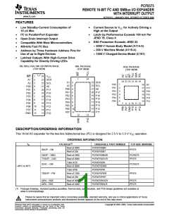
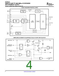
PCF8575
REMOTE 16-BIT I2C AND SMBus I/O EXPANDER
WITH INTERRUPT OUTPUT
www.ti.com
SCPS121C–JANUARY 2005–REVISED OCTOBER 2006
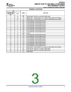
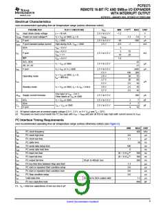
TERMINAL FUNCTIONS
NO.
DB, DBQ, DGV,
DW, PW, AND
RHL
NAME
FUNCTION
RGE
1
22
23
24
1
INT
A1
Interrupt output. Connect to VCC through a pullup resistor.
Address input 1. Connect directly to VCC or ground. Pullup resistors are not needed.
Address input 2. Connect directly to VCC or ground. Pullup resistors are not needed.
P-port input/output. Push-pull design structure.
P-port input/output. Push-pull design structure.
P-port input/output. Push-pull design structure.
P-port input/output. Push-pull design structure.
P-port input/output. Push-pull design structure.
P-port input/output. Push-pull design structure.
P-port input/output. Push-pull design structure.
P-port input/output. Push-pull design structure.
Ground
2
3
A2
4
P00
P01
P02
P03
P04
P05
P06
P07
GND
P10
P11
P12
P13
P14
P15
P16
P17
A0
5
2
6
3
7
4
8
5
9
6
10
11
12
13
14
15
16
17
18
19
20
21
22
23
24
7
8
9
10
11
12
13
14
15
16
17
18
19
20
21
P-port input/output. Push-pull design structure.
P-port input/output. Push-pull design structure.
P-port input/output. Push-pull design structure.
P-port input/output. Push-pull design structure.
P-port input/output. Push-pull design structure.
P-port input/output. Push-pull design structure.
P-port input/output. Push-pull design structure.
P-port input/output. Push-pull design structure.
Address input 0. Connect directly to VCC or ground. Pullup resistors are not needed.
Serial clock line. Connect to VCC through a pullup resistor
Serial data line. Connect to VCC through a pullup resistor.
Supply voltage
SCL
SDA
VCC
3
Submit Documentation Feedback

 TI [ TEXAS INSTRUMENTS ]