PCF8575
REMOTE 16-BIT I2C AND SMBus I/O EXPANDER
WITH INTERRUPT OUTPUT
www.ti.com
SCPS121C–JANUARY 2005–REVISED OCTOBER 2006
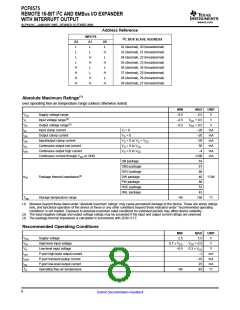
Address Reference
INPUTS
I2C BUS SLAVE ADDRESS
A2
L
A1
L
A0
L
32 (decimal), 20 (hexadecimal)
33 (decimal), 21 (hexadecimal)
34 (decimal), 22 (hexadecimal)
35 (decimal), 23 (hexadecimal)
36 (decimal), 24 (hexadecimal)
37 (decimal), 25 (hexadecimal)
38 (decimal), 26 (hexadecimal)
39 (decimal), 27 (hexadecimal)
L
L
H
L
L
H
H
L
L
H
L
H
H
H
H
L
H
L
H
H
H
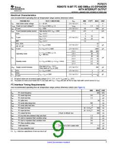
Absolute Maximum Ratings(1)
over operating free-air temperature range (unless otherwise noted)
MIN
–0.5
–0.5
–0.5
MAX
6.5
UNIT
VCC
VI
Supply voltage range
Input voltage range(2)
Output voltage range(2)
V
VCC + 0.5
VCC + 0.5
–20
–20
–20
50
V
VO
IIK
V
Input clamp current
VI < 0
mA
mA
mA
mA
mA
mA
IOK
IOK
IOL
IOH
Output clamp current
VO < 0
Input/output clamp current
Continuous output low current
Continuous output high current
Continuous current through VCC or GND
VO < 0 or VO > VCC
VO = 0 to VCC
VO = 0 to VCC
–4
±100
63
DB package
DBQ package
DGV package
DW package
PW package
RGE package
RHL package
61
86
θJA
Package thermal impedance(3)
46
°C/W
88
53
43
Tstg
Storage temperature range
–65
150
°C
(1) Stresses beyond those listed under "absolute maximum ratings" may cause permanent damage to the device. These are stress ratings
only, and functional operation of the device at these or any other conditions beyond those indicated under "recommended operating
conditions" is not implied. Exposure to absolute-maximum-rated conditions for extended periods may affect device reliability.
(2) The input negative-voltage and output voltage ratings may be exceeded if the input and output current ratings are observed.
(3) The package thermal impedance is calculated in accordance with JESD 51-7.
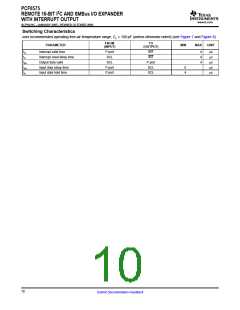
Recommended Operating Conditions
MIN
2.5
MAX
5.5
UNIT
V
VCC
VIH
VIL
Supply voltage
High-level input voltage
0.7 × VCC
–0.5
VCC + 0.5
0.3 × VCC
–1
V
Low-level input voltage
V
IOH
IOHT
IOL
P-port high-level output current
P-port transient pullup current
P-port low-level output current
Operating free-air temperature
mA
mA
mA
°C
–10
25
TA
–40
85
8
Submit Documentation Feedback

 TI [ TEXAS INSTRUMENTS ]