PCF8575
REMOTE 16-BIT I2C AND SMBus I/O EXPANDER
WITH INTERRUPT OUTPUT
www.ti.com
SCPS121C–JANUARY 2005–REVISED OCTOBER 2006
DESCRIPTION/ORDERING INFORMATION (CONTINUED)
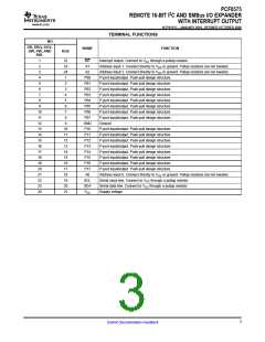
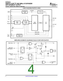
The PCF8575 provides general-purpose remote I/O expansion for most microcontroller families via the I2C
interface serial clock (SCL) and serial data (SDA).
The device features a 16-bit quasi-bidirectional input/output (I/O) port (P07–P00, P17–P10), including latched
outputs with high-current drive capability for directly driving LEDs. Each quasi-bidirectional I/O can be used as
an input or output without the use of a data-direction control signal. At power on, the I/Os are high. In this mode,
only a current source (IOH) to VCC is active. An additional strong pullup to VCC (IOHT) allows fast-rising edges into
heavily loaded outputs. This device turns on when an output is written high and is switched off by the negative
edge of SCL. The I/Os should be high before being used as inputs. After power on, as all the I/Os are set high,
all of them can be used as inputs. Any change in setting of the I/Os as either input or outputs can be done with
the write mode. If a high is applied externally to an I/O that has been written earlier to low, a large current (IOL
)
will flow to GND.
The PCF8575 provides an open-drain interrupt (INT) output, which can be connected to the interrupt input of a
microcontroller. An interrupt is generated by any rising or falling edge of the port inputs in the input mode. After
time, tiv, the signal INT is valid. Resetting and reactivating the interrupt circuit is achieved when data on the port
is changed to the original setting, or data is read from or written to the port that generated the interrupt.
Resetting occurs in the read mode at the acknowledge (ACK) bit after the rising edge of the SCL signal or in the
write mode at the ACK bit after the falling edge of the SCL signal. Interrupts that occur during the ACK clock
pulse can be lost (or be very short), due to the resetting of the interrupt during this pulse. Each change of the
I/Os after resetting is detected and is transmitted as INT. Reading from or writing to another device does not
affect the interrupt circuit.
By sending an interrupt signal on this line, the remote I/O can inform the microcontroller if there is incoming data
on its ports, without having to communicate via the I2C bus. Thus, the PCF8575 can remain a simple slave
device.
Every data transmission to or from the PCF8575 must consist of an even number of bytes. The first data byte in
every pair refers to port 0 (P07–P00), and the second data byte in every pair refers to port 1 (P17–P10). To
write to the ports (output mode), the master first addresses the slave device, setting the last bit of the byte
containing the slave address to logic 0. The PCF8575 acknowledges, and the master sends the first data byte
for P07–P00. After the first data byte is acknowledged by the PCF8575, the second data byte (P17–P10) is sent
by the master. Once again, the PCF8575 acknowledges the receipt of the data, after which this 16-bit data is
presented on the port lines.
The number of data bytes that can be sent successively is not limited. After every two bytes, the previous data is
overwritten. When the PCF8575 receives the pairs of data bytes, the first byte is referred to as P07–P00 and the
second byte as P17–P10. The third byte is referred to as P07–P00, the fourth byte as P17–P10, and so on.
Before reading from the PCF8575, all ports desired as input should be set to logic 1. To read from the ports
(input mode), the master first addresses the slave device, setting the last bit of the byte containing the slave
address to logic 1. The data bytes that follow on the SDA are the values on the ports. If the data on the input
port changes faster than the master can read, this data may be lost.
When power is applied to VCC, an internal power-on reset holds the PCF8575 in a reset state until VCC has
reached VPOR. At that time, the reset condition is released, and the device I2C-bus state machine initializes the
bus to its default state.
The hardware pins (A0, A1, and A2) are used to program and vary the fixed I2C address and allow up to eight
devices to share the same I2C bus or SMBus. The fixed I2C address of the PCF8575 is the same as the
PCF8575C, PCF8574, PCA9535, and PCA9555, allowing up to eight of these devices, in any combination, to
share the same I2C bus or SMBus.
2
Submit Documentation Feedback

 TI [ TEXAS INSTRUMENTS ]