OPA140
OPA2140, OPA4140
SBOS498A –JULY 2010–REVISED AUGUST 2010
www.ti.com
particular semiconductor fabrication process and
specific circuits connected to the pin. Additionally,
internal electrostatic discharge (ESD) protection is
built into these circuits to protect them from
accidental ESD events both before and during
product assembly.
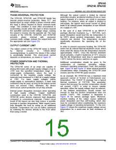
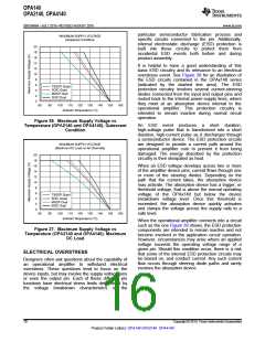
MAXIMUM SUPPLY VOLTAGE
(Quiescent Condition)
20
18
16
14
12
10
8
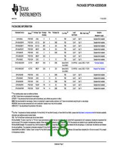
It is helpful to have a good understanding of this
basic ESD circuitry and its relevance to an electrical
overstress event. See Figure 38 for an illustration of
the ESD circuits contained in the OPAx140 series
(indicated by the dashed line area). The ESD
protection circuitry involves several current-steering
diodes connected from the input and output pins and
routed back to the internal power-supply lines, where
they meet at an absorption device internal to the
operational amplifier. This protection circuitry is
intended to remain inactive during normal circuit
operation.
6
TSSOP Quad
SOIC Quad
MSOP Dual
SOIC Dual
4
2
0
80
90
100
110
120
130
140
150
160
Ambient Temperature (?C)
Figure 36. Maximum Supply Voltage vs
Temperature (OPA2140 and OPA4140), Quiescent
Condition
An ESD event produces
a
short duration,
high-voltage pulse that is transformed into a short
duration, high-current pulse as it discharges through
a semiconductor device. The ESD protection circuits
are designed to provide a current path around the
operational amplifier core to prevent it from being
damaged. The energy absorbed by the protection
circuitry is then dissipated as heat.
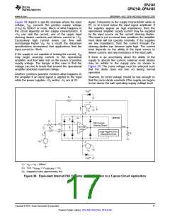
MAXIMUM SUPPLY VOLTAGE
(Maximum DC Load on All Channels)
20
18
16
14
12
10
8
When an ESD voltage develops across two or more
of the amplifier device pins, current flows through one
or more of the steering diodes. Depending on the
path that the current takes, the absorption device
may activate. The absorption device has a trigger, or
threshold voltage, that is above the normal operating
voltage of the OPAx140 but below the device
breakdown voltage level. Once this threshold is
exceeded, the absorption device quickly activates
and clamps the voltage across the supply rails to a
safe level.
6
TSSOP Quad
SOIC Quad
MSOP Dual
SOIC Dual
4
2
0
80
90
100
110
120
130
140
150
160
Ambient Temperature (?C)
When the operational amplifier connects into a circuit
such as the one Figure 38 shows, the ESD protection
components are intended to remain inactive and not
become involved in the application circuit operation.
However, circumstances may arise where an applied
voltage exceeds the operating voltage range of a
given pin. Should this condition occur, there is a risk
that some of the internal ESD protection circuits may
be biased on, and conduct current. Any such current
flow occurs through steering diode paths and rarely
involves the absorption device.
Figure 37. Maximum Supply Voltage vs
Temperature (OPA2140 and OPA4140), Maximum
DC Load
ELECTRICAL OVERSTRESS
Designers often ask questions about the capability of
an operational amplifier to withstand electrical
overstress. These questions tend to focus on the
device inputs, but may involve the supply voltage pins
or even the output pin. Each of these different pin
functions have electrical stress limits determined by
the voltage breakdown characteristics of the
16
Copyright © 2010, Texas Instruments Incorporated
Product Folder Link(s): OPA140 OPA2140 OPA4140

 TI [ TEXAS INSTRUMENTS ]