OPA140
OPA2140, OPA4140
SBOS498A –JULY 2010–REVISED AUGUST 2010
www.ti.com
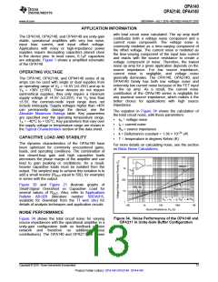
BASIC NOISE CALCULATIONS
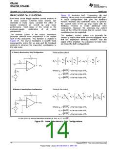
Figure 35 illustrates both noninverting (A) and
inverting (B) op amp circuit configurations with gain.
In circuit configurations with gain, the feedback
network resistors also contribute noise. In general,
the current noise of the op amp reacts with the
feedback resistors to create additional noise
components. However, the extremely low current
noise of the OPAx140 means that its current noise
contribution can be neglected.
Low-noise circuit design requires careful analysis of
all noise sources. External noise sources can
dominate in many cases; consider the effect of
source resistance on overall op amp noise
performance. Total noise of the circuit is the
root-sum-square
components.
combination
of
all
noise
The resistive portion of the source impedance
produces thermal noise proportional to the square
root of the resistance. This function is plotted in
Figure 34. The source impedance is usually fixed;
consequently, select the op amp and the feedback
resistors to minimize the respective contributions to
the total noise.
The feedback resistor values can generally be
chosen to make these noise sources negligible. Note
that low impedance feedback resistors load the
output of the amplifier. The equations for total noise
are shown for both configurations.
space
A) Noise in Noninverting Gain Configuration
Noise at the output:
R2
2
2
2
R2
R1
R2
R1
R2
R1
2
EO
2
en
2
2
es
e12 + e2
+
R1
1 +
1 +
=
+
EO
4kTRS
4kTR1
4kTR2
Where eS =
e1 =
= thermal noise of RS
= thermal noise of R1
= thermal noise of R2
RS
VS
e2 =
B) Noise in Inverting Gain Configuration
Noise at the output:
R2
2
2
2
R2
R2
R2
R1 + RS
EO2 = 1 +
2
2
2
en
+
e12 + e2
+
es
R1
R1 + RS
R1 + RS
EO
RS
4kTRS
4kTR1
4kTR2
Where eS =
e1 =
= thermal noise of RS
= thermal noise of R1
= thermal noise of R2
VS
e2 =
For the OPAx140 series of operational amplifiers at 1kHz, en = 5.1nV/√Hz.
Figure 35. Noise Calculation in Gain Configurations
14
Copyright © 2010, Texas Instruments Incorporated
Product Folder Link(s): OPA140 OPA2140 OPA4140

 TI [ TEXAS INSTRUMENTS ]