OPA140
OPA2140, OPA4140
www.ti.com
SBOS498A –JULY 2010–REVISED AUGUST 2010
PHASE-REVERSAL PROTECTION
Although the output current is limited by internal
protection circuitry, accidental shorting of one or more
output channels of a device can result in excessive
heating. For instance, when an output is shorted to
mid-supply, the typical short-circuit current of 36mA
leads to an internal power dissipation of over 600mW
at a supply of ±18V.
The OPA140, OPA2140, and OPA4140 family has
internal phase-reversal protection. Many FET- and
bipolar-input op amps exhibit a phase reversal when
the input is driven beyond its linear common-mode
range. This condition is most often encountered in
noninverting circuits when the input is driven beyond
the specified common-mode voltage range, causing
the output to reverse into the opposite rail. The input
circuitry of the OPA140, OPA2140, and OPA4140
In the case of a dual OPA2140 in an MSOP-8
package (thermal resistance qJA = 180°C/W), such
power dissipation would lead the die temperature to
be 220°C above ambient temperature, when both
channels are shorted. This temperature increase
significantly decreases the operating life of the
device.
prevents
phase
reversal
with
excessive
common-mode voltage; instead, the output limits into
the appropriate rail (see Figure 22).
OUTPUT CURRENT LIMIT
In order to prevent excessive heating, the OPAx140
series has an internal thermal shutdown circuit, which
shuts down the device if the die temperature exceeds
approximately +180°C. Once this thermal shutdown
circuit activates, a built-in hysteresis of 15°C ensures
that the die temperature must drop to approximately
+165°C before the device switches on again.
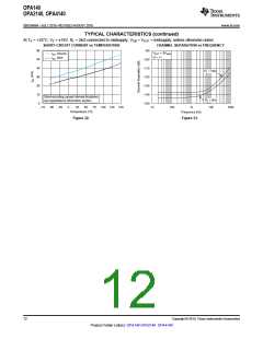
The output current of the OPAx140 series is limited
by
internal
circuitry
to
+36mA/–30mA
(sourcing/sinking), to protect the device if the output
is accidentally shorted. This short-circuit current
depends on temperature, as shown in Figure 32.
POWER DISSIPATION AND THERMAL
PROTECTION
Additional consideration should be given to the
combination of maximum operating voltage,
maximum operating temperature, load, and package
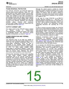
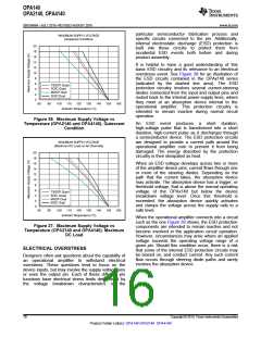
type. Figure 36 and Figure 37 show several practical
considerations when evaluating the OPA2140 (dual
version) and the OPA4140 (quad version).
The OPAx140 series of op amps are capable of
driving 2kΩ loads with power-supply voltages of up to
±18V over the specified temperature range. In a
single-supply configuration, where the load is
connected to the negative supply voltage, the
minimum load resistance is 2.8kΩ at a supply voltage
of +36V. For lower supply voltages (either
single-supply or symmetrical supplies), a lower load
resistance may be used, as long as the output current
does not exceed 13mA; otherwise, the device
short-circuit current protection circuit may activate.
As an example, the OPA4140 has a maximum total
quiescent current of 10.8mA (2.7mA/channel) over
temperature. The TSSOP-14 package has a typical
thermal resistance of 135°C/W. This parameter
means that because the junction temperature should
not exceed +150°C in order to ensure reliable
operation, either the supply voltage must be reduced,
or the ambient temperature should remain low
enough so that the junction temperature does not
exceed +150°C. This condition is illustrated in
Figure 36 for various package types. Moreover,
resistive loading of the output causes additional
power dissipation and thus self-heating, which also
must be considered when establishing the maximum
supply voltage or operating temperature. To this end,
Figure 37 shows the maximum supply voltage versus
temperature for a worst-case dc load resistance of
2kΩ.
Internal power dissipation increases when operating
at high supply voltages. Copper leadframe
construction used in the OPA140, OPA2140, and
OPA4140 series devices improves heat dissipation
compared to conventional materials. Printed circuit
board (PCB) layout can also help reduce a possible
increase in junction temperature. Wide copper traces
help dissipate the heat by acting as an additional
heatsink. Temperature rise can be further minimized
by soldering the devices directly to the PCB rather
than using a socket.
Copyright © 2010, Texas Instruments Incorporated
15
Product Folder Link(s): OPA140 OPA2140 OPA4140

 TI [ TEXAS INSTRUMENTS ]