MSP430F530x, MSP430F5310
SLAS677B –SEPTEMBER 2010–REVISED MARCH 2011
www.ti.com
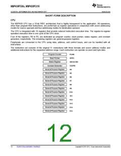
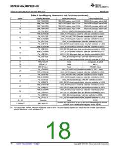
Interrupt Vector Addresses
The interrupt vectors and the power-up start address are located in the address range 0FFFFh to 0FF80h. The
vector contains the 16-bit address of the appropriate interrupt-handler instruction sequence.
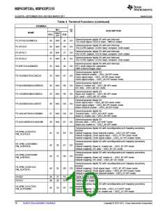
Table 4. Interrupt Sources, Flags, and Vectors
SYSTEM
INTERRUPT
WORD
ADDRESS
INTERRUPT SOURCE
INTERRUPT FLAG
PRIORITY
System Reset
Power-Up
External Reset
Watchdog Timeout, Password
Violation
(1) (2)
WDTIFG, KEYV (SYSRSTIV)
Reset
0FFFEh
63, highest
Flash Memory Password Violation
System NMI
PMM
Vacant Memory Access
JTAG Mailbox
SVMLIFG, SVMHIFG, DLYLIFG, DLYHIFG,
VLRLIFG, VLRHIFG, VMAIFG, JMBNIFG,
(Non)maskable
(Non)maskable
0FFFCh
0FFFAh
62
61
(1)
JMBOUTIFG (SYSSNIV)
User NMI
NMI
Oscillator Fault
NMIIFG, OFIFG, ACCVIFG, BUSIFG (SYSUNIV)
(1) (2)
Flash Memory Access Violation
(1) (3)
Comp_B
TB0
Comparator B interrupt flags (CBIV)
Maskable
Maskable
0FFF8h
0FFF6h
60
59
(3)
TB0CCR0 CCIFG0
TB0CCR1 CCIFG1 to TB0CCR6 CCIFG6,
TB0
Maskable
Maskable
0FFF4h
0FFF2h
58
57
(1) (3)
TB0IFG (TB0IV)
Watchdog Timer_A Interval Timer
Mode
WDTIFG
(1) (3)
USCI_A0 Receive/Transmit
USCI_B0 Receive/Transmit
ADC10_A
UCA0RXIFG, UCA0TXIFG (UCA0IV)
Maskable
Maskable
Maskable
Maskable
0FFF0h
0FFEEh
0FFECh
0FFEAh
56
55
54
53
(1) (3)
UCB0RXIFG, UCB0TXIFG (UCAB0IV)
(1) (3) (4)
ADC10IFG0
(3)
TA0
TA0CCR0 CCIFG0
TA0CCR1 CCIFG1 to TA0CCR4 CCIFG4,
TA0
Maskable
0FFE8h
52
(1) (3)
TA0IFG (TA0IV)
LDO-PWR
DMA
LDOOFFIG, LDOONIFG, LDOOVLIFG
Maskable
Maskable
Maskable
0FFE6h
0FFE4h
0FFE2h
51
50
49
(1) (3)
DMA0IFG, DMA1IFG, DMA2IFG (DMAIV)
(3)
TA1
TA1CCR0 CCIFG0
TA1CCR1 CCIFG1 to TA1CCR2 CCIFG2,
TA1
Maskable
0FFE0h
48
(1) (3)
TA1IFG (TA1IV)
(1) (3)
I/O Port P1
USCI_A1 Receive/Transmit
USCI_B1 Receive/Transmit
TA2
P1IFG.0 to P1IFG.7 (P1IV)
Maskable
Maskable
Maskable
Maskable
0FFDEh
0FFDCh
0FFDAh
0FFD8h
47
46
45
44
(1) (3)
UCA1RXIFG, UCA1TXIFG (UCA1IV)
(1) (3)
UCB1RXIFG, UCB1TXIFG (UCB1IV)
(3)
TA2CCR0 CCIFG0
TA2CCR1 CCIFG1 to TA2CCR2 CCIFG2,
TA2
Maskable
Maskable
Maskable
0FFD6h
0FFD4h
0FFD2h
43
42
41
(1) (3)
TA2IFG (TA2IV)
(1) (3)
I/O Port P2
RTC_A
P2IFG.0 to P2IFG.7 (P2IV)
RTCRDYIFG, RTCTEVIFG, RTCAIFG,
(1) (3)
RT0PSIFG, RT1PSIFG (RTCIV)
0FFD0h
⋮
40
(5)
Reserved
Reserved
⋮
0FF80h
0, lowest
(1) Multiple source flags
(2) A reset is generated if the CPU tries to fetch instructions from within peripheral space or vacant memory space.
(Non)maskable: the individual interrupt-enable bit can disable an interrupt event, but the general-interrupt enable cannot disable it.
(3) Interrupt flags are located in the module.
(4) Only on devices with ADC, otherwise reserved.
(5) Reserved interrupt vectors at addresses are not used in this device and can be used for regular program code if necessary. To maintain
compatibility with other devices, it is recommended to reserve these locations.
14
Submit Documentation Feedback
Copyright © 2010–2011, Texas Instruments Incorporated

 TI [ TEXAS INSTRUMENTS ]