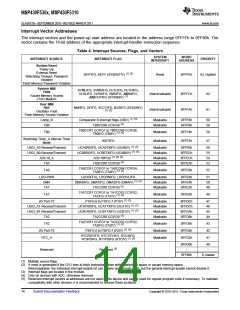
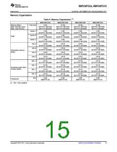
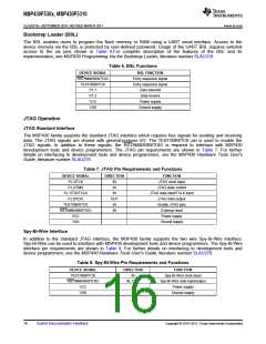
MSP430F530x, MSP430F5310
SLAS677B –SEPTEMBER 2010–REVISED MARCH 2011
www.ti.com
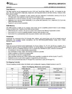
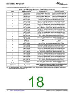
Table 9. Port Mapping, Mnemonics and Functions (continued)
Value
PxMAPy Mnemonic
PM_TB0CCR3A
PM_TB0CCR4A
PM_TB0CCR5A
PM_TB0CCR6A
PM_UCA1RXD
PM_UCA1SOMI
PM_UCA1TXD
PM_UCA1SIMO
PM_UCA1CLK
PM_UCB1STE
PM_UCB1SOMI
PM_UCB1SCL
PM_UCB1SIMO
PM_UCB1SDA
PM_UCB1CLK
PM_UCA1STE
PM_CBOUT1
Input Pin Function
Output Pin Function
7
8
TB0 CCR3 capture input CCI3A
TB0 CCR4 capture input CCI4A
TB0 CCR5 capture input CCI5A
TB0 CCR6 capture input CCI6A
TB0 CCR3 compare output Out3
TB0 CCR4 compare output Out4
TB0 CCR5 compare output Out5
TB0 CCR6 compare output Out6
9
10
USCI_A1 UART RXD (Direction controlled by USCI - input)
USCI_A1 SPI slave out master in (direction controlled by USCI)
USCI_A1 UART TXD (Direction controlled by USCI - output)
USCI_A1 SPI slave in master out (direction controlled by USCI)
USCI_A1 clock input/output (direction controlled by USCI)
USCI_B1 SPI slave transmit enable (direction controlled by USCI)
USCI_B1 SPI slave out master in (direction controlled by USCI)
USCI_B1 I2C clock (open drain and direction controlled by USCI)
USCI_B1 SPI slave in master out (direction controlled by USCI)
USCI_B1 I2C data (open drain and direction controlled by USCI)
USCI_B1 clock input/output (direction controlled by USCI)
USCI_A1 SPI slave transmit enable (direction controlled by USCI)
11
12
13
14
15
16
17
18
19
None
None
None
Comparator_B output
MCLK
PM_MCLK
PM_RTCCLK
RTCCLK output
PM_UCA0RXD
PM_UCA0SOMI
PM_UCA0TXD
PM_UCA0SIMO
PM_UCA0CLK
PM_UCB0STE
PM_UCB0SOMI
PM_UCB0SCL
PM_UCB0SIMO
PM_UCB0SDA
PM_UCB0CLK
PM_UCA0STE
Reserved
USCI_A0 UART RXD (Direction controlled by USCI - input)
USCI_A0 SPI slave out master in (direction controlled by USCI)
USCI_A0 UART TXD (Direction controlled by USCI - output)
USCI_A0 SPI slave in master out (direction controlled by USCI)
USCI_A0 clock input/output (direction controlled by USCI)
USCI_B0 SPI slave transmit enable (direction controlled by USCI)
USCI_B0 SPI slave out master in (direction controlled by USCI)
USCI_B0 I2C clock (open drain and direction controlled by USCI)
USCI_B0 SPI slave in master out (direction controlled by USCI)
USCI_B0 I2C data (open drain and direction controlled by USCI)
USCI_B0 clock input/output (direction controlled by USCI)
USCI_A0 SPI slave transmit enable (direction controlled by USCI)
20
21
22
23
24
25
26 - 30
None
DVSS
Disables the output driver as well as the input Schmitt-trigger to prevent
parasitic cross currents when applying analog signals.
(1)
31 (0FFh)
PM_ANALOG
(1) The value of the PMPAP_ANALOG mnemonic is set to 0FFh. The port mapping registers are only 5 bits wide and the upper bits are
ignored resulting in a read out value of 31.
18
Submit Documentation Feedback
Copyright © 2010–2011, Texas Instruments Incorporated

 TI [ TEXAS INSTRUMENTS ]