MSP430G2x53
MSP430G2x13
www.ti.com
SLAS735A –APRIL 2011–REVISED MAY 2011
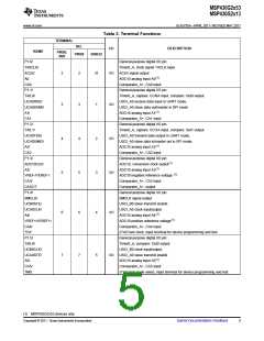
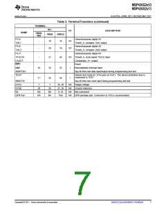
Table 2. Terminal Functions (continued)
TERMINAL
NO.
I/O
DESCRIPTION
NAME
PW20,
N20
PW28
RHB32
P3.5/
General-purpose digital I/O
Timer0_A, compare: Out1 output
General-purpose digital I/O
Timer0_A, compare: Out2 output
General-purpose digital I/O
Timer0_A, clock signal TACLK input
Comparator_A+, output
-
-
19
20
18
I/O
I/O
TA0.1
P3.6/
19
20
TA0.2
P3.7/
TA1CLK/
CAOUT
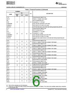
RST/
-
21
I/O
Reset
NMI/
16
17
24
25
23
24
I
I
Nonmaskable interrupt input
SBWTDIO
TEST/
Spy-Bi-Wire test data input/output during programming and test
Selects test mode for JTAG pins on Port 1. The device protection fuse is
connected to TEST.
SBWTCK
DVCC
DVSS
Spy-Bi-Wire test clock input during programming and test
Supply voltage
1
1
29, 30
27, 28
8, 32
Pad
NA
NA
NA
NA
20
NA
NA
28
NA
NA
Ground reference
NC
Not connected
QFN Pad
QFN package pad. Connection to VSS is recommended.
Copyright © 2011, Texas Instruments Incorporated
Submit Documentation Feedback
7

 TI [ TEXAS INSTRUMENTS ]