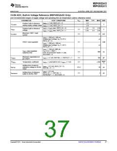
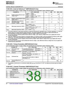
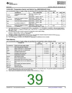
MSP430G2x53
MSP430G2x13
www.ti.com
SLAS735A –APRIL 2011–REVISED MAY 2011
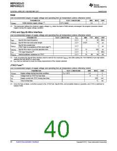
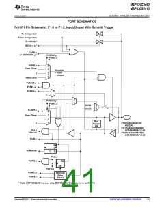
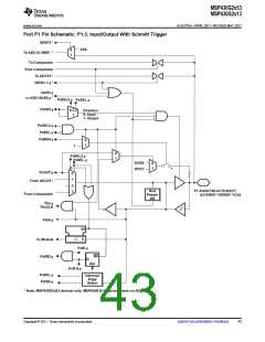
PORT SCHEMATICS
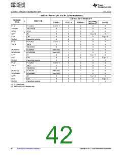
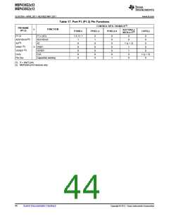
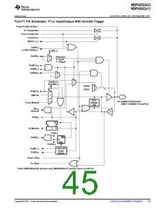
Port P1 Pin Schematic: P1.0 to P1.2, Input/Output With Schmitt Trigger
To Comparator
From Comparator
To ADC10 *
INCHx = y *
CAPD.y
or ADC10AE0.y *
PxSEL2.y
PxSEL.y
PxDIR.y
0
From Timer
1
Direction
0: Input
1: Output
1
2
3
From USCI
PxSEL2.y
PxSEL.y
PxREN.y
0
1
1
0
1
PxSEL2.y
PxSEL.y
DVSS
DVCC
0
1
1
PxOUT.y
0
1
From Timer
2
3
Bus
Keeper
EN
P1.0/TA0CLK/ACLK/
A0*/CA0
0
P1.1/TA0.0/UCA0RXD/
UCA0SOMI/A1*/CA1
P1.2/TA0.1/UCA0TXD/
UCA0SIMO/A2*/CA2
TAx.y
TAxCLK
PxIN.y
EN
To Module
PxIRQ.y
D
PxIE.y
EN
Set
Q
PxIFG.y
PxSEL.y
PxIES.y
Interrupt
Edge
Select
* Note: MSP430G2x53 devices only. MSP430G2x13 devices have no ADC10.
Copyright © 2011, Texas Instruments Incorporated
Submit Documentation Feedback
41

 TI [ TEXAS INSTRUMENTS ]