MSP430G2x53
MSP430G2x13
SLAS735A –APRIL 2011–REVISED MAY 2011
www.ti.com
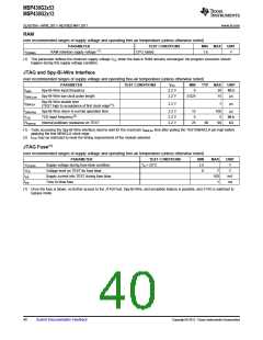
RAM
over recommended ranges of supply voltage and operating free-air temperature (unless otherwise noted)
PARAMETER
TEST CONDITIONS
CPU halted
MIN
MAX
UNIT
(1)
V(RAMh)
RAM retention supply voltage
1.6
V
(1) This parameter defines the minimum supply voltage VCC when the data in RAM remains unchanged. No program execution should
happen during this supply voltage condition.
JTAG and Spy-Bi-Wire Interface
over recommended ranges of supply voltage and operating free-air temperature (unless otherwise noted)
PARAMETER
TEST CONDITIONS
VCC
MIN
0
TYP
MAX
20
UNIT
MHz
µs
fSBW
Spy-Bi-Wire input frequency
2.2 V
2.2 V
tSBW,Low Spy-Bi-Wire low clock pulse length
0.025
15
Spy-Bi-Wire enable time
tSBW,En
2.2 V
1
µs
(TEST high to acceptance of first clock edge(1)
)
tSBW,Ret
fTCK
Spy-Bi-Wire return to normal operation time
TCK input frequency(2)
2.2 V
2.2 V
2.2 V
15
0
100
5
µs
MHz
kΩ
RInternal
Internal pulldown resistance on TEST
25
60
90
(1) Tools accessing the Spy-Bi-Wire interface need to wait for the maximum tSBW,En time after pulling the TEST/SBWCLK pin high before
applying the first SBWCLK clock edge.
(2) fTCK may be restricted to meet the timing requirements of the module selected.
JTAG Fuse(1)
over recommended ranges of supply voltage and operating free-air temperature (unless otherwise noted)
PARAMETER
TEST CONDITIONS
TA = 25°C
MIN
2.5
6
MAX
UNIT
V
VCC(FB)
VFB
Supply voltage during fuse-blow condition
Voltage level on TEST for fuse blow
Supply current into TEST during fuse blow
Time to blow fuse
7
100
1
V
IFB
mA
ms
tFB
(1) Once the fuse is blown, no further access to the JTAG/Test, Spy-Bi-Wire, and emulation feature is possible, and JTAG is switched to
bypass mode.
40
Submit Documentation Feedback
Copyright © 2011, Texas Instruments Incorporated

 TI [ TEXAS INSTRUMENTS ]