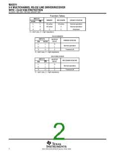
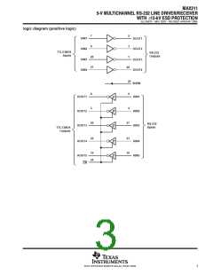
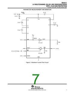
ꢀ ꢁ ꢂ ꢃꢄꢄ
ꢅꢆ ꢇ ꢀ ꢈꢉꢊ ꢋ ꢌ ꢍꢁ ꢎ ꢎꢏꢉ ꢐꢑ ꢆꢃ ꢒ ꢃ ꢉꢋ ꢎ ꢏ ꢓꢐ ꢋ ꢇꢏ ꢐꢔꢐꢏ ꢌꢏꢋ ꢇꢏꢐ
ꢕꢋ ꢊ ꢍ ꢄ ꢅꢆ ꢖꢇ ꢏꢑ ꢓ ꢗ ꢐꢘ ꢊꢏ ꢌꢊꢋ ꢘ ꢎ
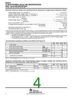
SLLS567E − MAY 2003 − REVISED JANUARY 2004
RECEIVER SECTION
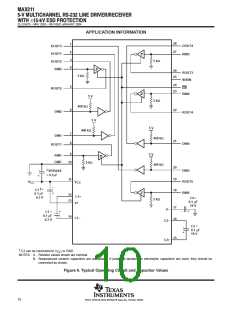
electrical characteristics over recommended ranges of supply voltage and operating free-air
temperature (unless otherwise noted) (see Note 4 and Figure 6)
†
PARAMETER
High-level output voltage
TEST CONDITIONS
= −1 mA
MIN
TYP
MAX
UNIT
V
V
OH
V
OL
V
IT+
V
IT−
V
hys
I
I
3.5
V −0.4V
CC
OH
Low-level output voltage
= 1.6 mA
0.4
2.4
V
OL
Positive-going input threshold voltage
Negative-going input threshold voltage
V
= 5 V,
= 5 V,
T
= 25°C
= 25°C
1.7
1.2
0.5
5
V
CC
CC
A
V
T
A
0.8
0.2
3
V
Input hysteresis (V
− V
)
1
7
V
IT+
IT−
r
Input resistance
V
= 5 V,
T = 25°C
A
kW
µA
i
CC
Output leakage current
EN = V
CC
,
0 ≤ ROUT ≤ V
CC
0.05
10
†
All typical values are at V = 5 V, and T = 25°C.
CC
A
NOTE 4: Test conditions are C1−C4 = 0.1 µF at V
= 5 V 0.5 V.
CC
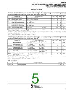
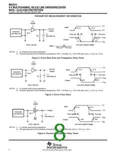
switching characteristics over recommended ranges of supply voltage and operating free-air
temperature (unless otherwise noted) (see Note 4)
†
PARAMETER
TEST CONDITIONS
MIN TYP
MAX
10
UNIT
µs
t
t
Propagation delay time, low- to high-level output
Propagation delay time, high- to low-level output
C = 150 pF,
See Figure 4
See Figure 4
0.5
0.5
PLH (R)
L
C = 150 pF,
10
µs
PHL (R)
L
C = 150 pF,
L
R
= 1 kΩ,
L
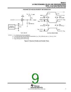
t
Output enable time
Output disable time
600
ns
en
See Figure 5
C = 150 pF,
L
See Figure 5
R
= 1 kΩ,
L
t
t
200
300
ns
ns
dis
‡
Pulse skew
See Figure 3
sk(p)
†
‡
All typical values are at V
CC
= 5 V, and T = 25°C.
A
Pulse skew is defined as |t
− t | of each channel of the same device.
PLH PHL
NOTE 4: Test conditions are C1−C4 = 0.1 µF, at V
= 5 V 0.5 V.
CC
6
POST OFFICE BOX 655303 • DALLAS, TEXAS 75265

 TI [ TEXAS INSTRUMENTS ]