ꢀ ꢁꢂ ꢃ ꢄꢄ
ꢅ ꢆꢇ ꢀ ꢈꢉꢊ ꢋꢌꢍ ꢁꢎꢎꢏꢉ ꢐꢑ ꢆꢃꢒ ꢃ ꢉ ꢋꢎꢏ ꢓꢐꢋ ꢇꢏ ꢐꢔꢐꢏ ꢌꢏ ꢋ ꢇ ꢏꢐ
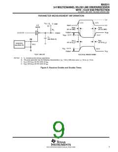
ꢕ ꢋꢊ ꢍ ꢄ ꢅ ꢆꢖ ꢇ ꢏꢑ ꢓ ꢗꢐ ꢘ ꢊꢏ ꢌꢊ ꢋꢘ ꢎ
SLLS567E − MAY 2003 − REVISED JANUARY 2004
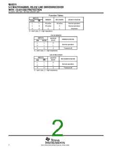
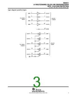
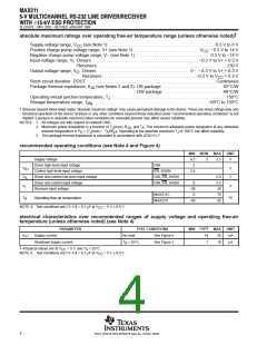
DRIVER SECTION
electrical characteristics over recommended ranges of supply voltage and operating free-air
temperature (unless otherwise noted) (see Note 4 and Figure 4)
†
PARAMETER
TEST CONDITIONS
DOUT at R = 3 kΩ to GND
MIN TYP
MAX
UNIT
V
V
V
High-level output voltage
Low-level output voltage
5
9
OH
L
DOUT at R = 3 kΩ to GND
−5
−9
15
3
V
OL
L
Driver high-level input current
Control high-level input current
Driver low-level input current
Control low-level input current
DIN = V
CC
200
10
I
IH
µA
µA
EN, SHDN = V
CC
DIN = 0 V
−15 −200
I
I
IL
EN, SHDN = 0 V
−3
10
−10
60
‡
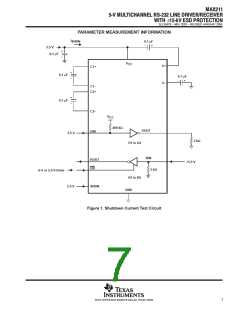
Short-circuit output current
Output resistance
V
V
= 5.5 V,
V
V
= 0 V
mA
OS
CC
O
r
, V+, and V− = 0 V,
=
2 V
300
W
o
CC
O
†
‡
All typical values are at V
CC
= 5 V, and T = 25°C.
A
Short-circuit durations should be controlled to prevent exceeding the device absolute power dissipation ratings, and not more than one output
should be shorted at a time.
NOTE 4: Test conditions are C1−C4 = 0.1 µF at V
CC
= 5 V 0.5 V.
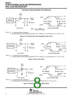
switching characteristics over recommended ranges of supply voltage and operating free-air
temperature (unless otherwise noted) (see Note 4)
†
PARAMETER
TEST CONDITIONS
MIN TYP
MAX
UNIT
C
= 50 pF to 1000 pF, = 3 kΩ to 7 kΩ,
R
L
L
Maximum data rate
120
kbit/s
One DOUT switching,
See Figure 2
R = 3 kΩ,
L
Propagation delay time,
low- to high-level output
C
= 2500 pF,
L
t
t
t
2
2
µs
µs
PLH (D)
PHL (D)
sk(p)
All drivers loaded,
See Figure 2
Propagation delay time,
high- to low-level output
C
= 2500 pF,
R
L
= 3 kΩ,
See Figure 2
L
All drivers loaded,
C
= 150 pF to 2500 pF,
R
L
= 3 kΩ to 7 kΩ,
L
§
Pulse skew
300
6
ns
See Figure 3
R = 3 kΩ to 7 kΩ,
L
Slew rate, transition region
(see Figure 2)
C
= 50 pF to 1000 pF,
= 5 V
L
SR(tr)
3
30
V/µs
V
CC
†
§
All typical values are at V
CC
= 5 V, and T = 25°C.
A
Pulse skew is defined as |t
− t | of each channel of the same device.
PLH PHL
NOTE 4: Test conditions are C1−C4 = 0.1 µF at V
= 5 V 0.5 V.
CC
ESD protection
PIN
TEST CONDITIONS
TYP
UNIT
D
, R
OUT IN
Human-Body Model
15
kV
5
POST OFFICE BOX 655303 • DALLAS, TEXAS 75265

 TI [ TEXAS INSTRUMENTS ]