ꢀ ꢁ ꢂ ꢃꢄꢄ
ꢅꢆ ꢇ ꢀ ꢈꢉꢊ ꢋ ꢌ ꢍꢁ ꢎ ꢎꢏꢉ ꢐꢑ ꢆꢃ ꢒ ꢃ ꢉꢋ ꢎ ꢏ ꢓꢐ ꢋ ꢇꢏ ꢐꢔꢐꢏ ꢌꢏꢋ ꢇꢏꢐ
ꢕꢋ ꢊ ꢍ ꢄ ꢅꢆ ꢖꢇ ꢏꢑ ꢓ ꢗ ꢐꢘ ꢊꢏ ꢌꢊꢋ ꢘ ꢎ
SLLS567E − MAY 2003 − REVISED JANUARY 2004
†
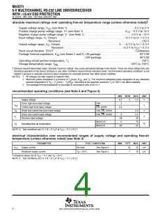
absolute maximum ratings over operating free-air temperature range (unless otherwise noted)
Supply voltage range, V
Positive charge pump voltage range, V+ (see Note 1) . . . . . . . . . . . . . . . . . . . . . . . . . . . . V
Negative charge pump voltage range, V− (see Note 1) . . . . . . . . . . . . . . . . . . . . . . . . . . . . . . . . . 0.3 V to −14 V
(see Note 1) . . . . . . . . . . . . . . . . . . . . . . . . . . . . . . . . . . . . . . . . . . . . . . −0.3 V to 6 V
CC
− 0.3 V to 14 V
CC
Input voltage range, V : Drivers . . . . . . . . . . . . . . . . . . . . . . . . . . . . . . . . . . . . . . . . . . . . . . . . −0.3 V to V+ + 0.3 V
I
Receivers . . . . . . . . . . . . . . . . . . . . . . . . . . . . . . . . . . . . . . . . . . . . . . . . . . . . . . . . . . 30 V
Output voltage range, V : Drivers . . . . . . . . . . . . . . . . . . . . . . . . . . . . . . . . . . . . . . . . V− − 0.3 V to V+ + 0.3 V
O
Receivers . . . . . . . . . . . . . . . . . . . . . . . . . . . . . . . . . . . . . . . . . . −0.3 V to V
+ 0.3 V
CC
Short-circuit duration: DOUT . . . . . . . . . . . . . . . . . . . . . . . . . . . . . . . . . . . . . . . . . . . . . . . . . . . . . . . . . . Continuous
Package thermal impedance, θ (see Notes 2 and 3): DB package . . . . . . . . . . . . . . . . . . . . . . . . . . . 62°C/W
JA
DW package . . . . . . . . . . . . . . . . . . . . . . . . . . 46°C/W
Operating virtual junction temperature, T . . . . . . . . . . . . . . . . . . . . . . . . . . . . . . . . . . . . . . . . . . . . . . . . . . . 150°C
J
Storage temperature range, T
. . . . . . . . . . . . . . . . . . . . . . . . . . . . . . . . . . . . . . . . . . . . . . . . . . . −65°C to 150°C
stg
†
Stresses beyond those listed under “absolute maximum ratings” may cause permanent damage to the device. These are stress ratings only, and
functional operation of the device at these or any other conditions beyond those indicated under “recommended operating conditions” is not
implied. Exposure to absolute-maximum-rated conditions for extended periods may affect device reliability.
NOTES: 1. All voltages are with respect to network GND.
2. Maximum power dissipation is a function of T (max), θ , and T . The maximum allowable power dissipation at any allowable
J
JA
A
ambient temperature is P = (T (max) − T )/θ . Operating at the absolute maximum T of 150°C can affect reliability.
D
J
A
JA
J
3. The package thermal impedance is calculated in accordance with JESD 51-7.
recommended operating conditions (see Note 4 and Figure 4)
MIN NOM
MAX
UNIT
Supply voltage
4.5
2
5
5.5
V
Driver high-level input voltage
Control high-level input voltage
Driver and control low-level input voltage
Driver and control input voltage
Receiver input voltage
DIN
V
V
V
V
IH
EN, SHDN
2.4
DIN, EN, SHDN
DIN, EN, SHDN
0.8
5.5
30
70
85
IL
0
−30
0
V
I
V
MAX211C
MAX211I
T
A
Operating free-air temperature
°C
−40
NOTE 4: Test conditions are C1−C4 = 0.1 µF at V
CC
= 5 V 0.5 V.
electrical characteristics over recommended ranges of supply voltage and operating free-air
temperature (unless otherwise noted) (see Note 4)
‡
PARAMETER
TEST CONDITIONS
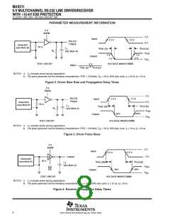
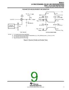
See Figure 6
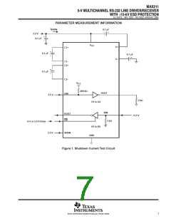
See Figure 1
MIN TYP
MAX
20
UNIT
mA
I
Supply current
Shutdown supply current
All typical values are at V = 5 V, and T = 25°C.
No load,
= 25°C,
14
1
CC
T
A
10
µA
‡
CC
A
NOTE 4: Test conditions are C1−C4 = 0.1 µF at V
= 5 V 0.5 V.
CC
4
POST OFFICE BOX 655303 • DALLAS, TEXAS 75265

 TI [ TEXAS INSTRUMENTS ]