LMH0324
www.ti.com.cn
ZHCSIC8B –APRIL 2016–REVISED JUNE 2018
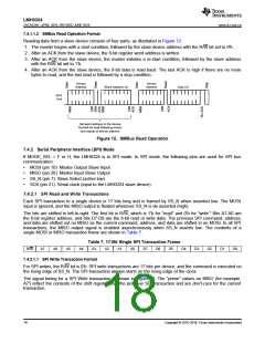
tSSOF
tSSH
SS_N
tPL
tSSSU
tPH
SCK
tH
tSU
HiZ
MOSI
0
A7
A6
A5
A4
A3
A2
A1
A0
D7
D6
D5
D4
D3
D2
D1
D0
tODZ
HiZ
MISO
R/W
A7'
A6'
A5'
A4'
A3'
A2'
A1'
A0'
D7'
D6'
D5'
D4'
D3'
D2'
D1'
D0'
Figure 13. Signal Timing for a SPI Write Transaction
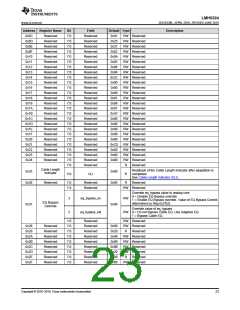
7.4.2.1.2 SPI Read Transaction Format
A SPI read transaction is 34 bits per device and consists of two 17-bit frames. The first 17-bit read transaction
frame shifts in the address to be read, followed by a dummy transaction second frame to shift out 17-bit read
data. The R/W bit is 1'b for the read transaction, as shown in Figure 14.
The first 17 bits from the read transaction specifies 1-bit of R/W and 8-bits of address A7-A0 in the first 8 bits.
The eight 1’s following the address are ignored. The second dummy transaction acts like a read operation on
address 0xFF and needs to be ignored. However, the transaction is necessary in order to shift out the read data
D7-D0 in the last 8 bits of the MISO output. As with the SPI Write, the “prime” values on MISO during the first 16
clocks are don’t-care for this portion of the transaction. The values shifted out on MISO during the last 17 clocks
reflect the read address and 8-bit read data for the current transaction.
tSSOF
SS_N
(host)
tSSOF
tSSSU
tPH
tPL
tSSH
SCK
(host)
tH
—8X1“
—17X1“
tSU
MOSI
(host)
A7 A6 A5 A4 A3 A2 A1 A0
1
tOD
tODZ
tOZD
MISO
(device)
A7' A6' A5' A4' A3' A2' A1' A0' D7' D6' D5' D4' D3' D2' D1' D0'
1
Don‘t Care
Figure 14. Signal Timing for a SPI Read Transaction
Copyright © 2016–2018, Texas Instruments Incorporated
19

 TI [ TEXAS INSTRUMENTS ]