DAC081S101
SNAS323C –JUNE 2005–REVISED FEBRUARY 2013
www.ti.com
DSP/MICROPROCESSOR INTERFACING
Interfacing the DAC081S101 to microprocessors and DSPs is quite simple. The following guidelines are offered
to hasten the design process.
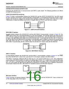
ADSP-2101/ADSP2103 Interfacing
Figure 37 shows a serial interface between the DAC081S101 and the ADSP-2101/ADSP2103. The DSP should
be set to operate in the SPORT Transmit Alternate Framing Mode. It is programmed through the SPORT control
register and should be configured for Internal Clock Operation, Active Low Framing and 16-bit Word Length.
Transmission is started by writing a word to the Tx register after the SPORT mode has been enabled.
ADSP-2101/
DAC081S101
ADSP2103
SYNC
DIN
SCLK
TFS
DT
SCLK
Figure 37. ADSP-2101/2103 Interface
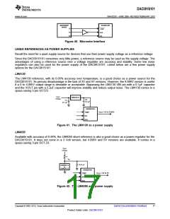
80C51/80L51 Interface
A serial interface between the DAC081S101 and the 80C51/80L51 microcontroller is shown in Figure 38. The
SYNC signal comes from a bit-programmable pin on the microcontroller. The example shown here uses port line
P3.3. This line is taken low when data is to transmitted to the DAC081S101. Since the 80C51/80L51 transmits 8-
bit bytes, only eight falling clock edges occur in the transmit cycle. To load data into the DAC, the P3.3 line must
be left low after the first eight bits are transmitted. A second write cycle is initiated to transmit the second byte of
data, after which port line P3.3 is brought high. The 80C51/80L51 transmit routine must recognize that the
80C51/80L51 transmits data with the LSB first while the DAC081S101 requires data with the MSB first.
80C51/80L51
P3.3
DAC081S101
SYNC
TXD
RXD
SCLK
DIN
Figure 38. 80C51/80L51 Interface
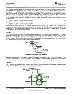
68HC11 Interface
A serial interface between the DAC081S101 and the 68HC11 microcontroller is shown in Figure 39. The SYNC
line of the DAC081S101 is driven from a port line (PC7 in the figure), similar to the 80C51/80L51.
The 68HC11 should be configured with its CPOL bit as a zero and its CPHA bit as a one. This configuration
causes data on the MOSI output to be valid on the falling edge of SCLK. PC7 is taken low to transmit data to the
DAC. The 68HC11 transmits data in 8-bit bytes with eight falling clock edges. Data is transmitted with the MSB
first. PC7 must remain low after the first eight bits are transferred. A second write cycle is initiated to transmit the
second byte of data to the DAC, after which PC7 should be raised to end the write sequence.
68HC11
DAC081S101
SYNC
PC7
SCK
SCLK
MOSI
DIN
Figure 39. 68HC11 Interface
Microwire Interface
Figure 40 shows an interface between a Microwire compatible device and the DAC081S101. Data is clocked out
on the rising edges of the SCLK signal.
16
Submit Documentation Feedback
Copyright © 2005–2013, Texas Instruments Incorporated
Product Folder Links: DAC081S101

 TI [ TEXAS INSTRUMENTS ]