DAC081S101
www.ti.com
SNAS323C –JUNE 2005–REVISED FEBRUARY 2013
Like any low dropout regulator, the LP2980 requires an output capacitor for loop stability. This output capacitor
must be at least 1.0µF over temperature, but values of 2.2µF or more will provide even better performance. The
ESR of this capacitor should be within the range specified in the LP2980 data sheet. Surface-mount solid
tantalum capacitors offer a good combination of small size and ESR. Ceramic capacitors are attractive due to
their small size but generally have ESR values that are too low for use with the LP2980. Aluminum electrolytic
capacitors are typically not a good choice due to their large size and have ESR values that may be too high at
low temperatures.
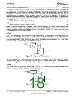
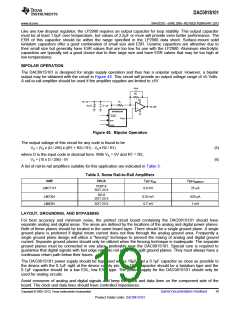
BIPOLAR OPERATION
The DAC081S101 is designed for single supply operation and thus has a unipolar output. However, a bipolar
output may be obtained with the circuit in Figure 45. This circuit will provide an output voltage range of ±5 Volts.
A rail-to-rail amplifier should be used if the amplifier supplies are limited to ±5V.
10 pF
R
2
+5V
+5V
R
1
+
-
10 mF
0.1 mF
±5V
+
DAC081S101
-5V
SYNC
V
OUT
DIN
SCLK
Figure 45. Bipolar Operation
The output voltage of this circuit for any code is found to be
VO = (VA x (D / 256) x ((R1 + R2) / R1) - VA x R2 / R1)
(5)
(6)
where D is the input code in decimal form. With VA = 5V and R1 = R2,
VO = (10 x D / 256) - 5V
A list of rail-to-rail amplifiers suitable for this application are indicated in Table 3.
Table 3. Some Rail-to-Rail Amplifiers
AMP
PKGS
Typ VOS
Typ ISUPPLY
PDIP-8
SOT-23-5
LMC7111
0.9 mV
25 µA
SO-8
SOT-23-5
LM7301
LM8261
0.03 mV
0.7 mV
620 µA
1 mA
SOT-23-5
LAYOUT, GROUNDING, AND BYPASSING
For best accuracy and minimum noise, the printed circuit board containing the DAC081S101 should have
separate analog and digital areas. The areas are defined by the locations of the analog and digital power planes.
Both of these planes should be located in the same board layer. There should be a single ground plane. A single
ground plane is preferred if digital return current does not flow through the analog ground area. Frequently a
single ground plane design will utilize a "fencing" technique to prevent the mixing of analog and digital ground
current. Separate ground planes should only be utilized when the fencing technique is inadequate. The separate
ground planes must be connected in one place, preferably near the DAC081S101. Special care is required to
guarantee that digital signals with fast edge rates do not pass over split ground planes. They must always have a
continuous return path below their traces.
The DAC081S101 power supply should be bypassed with a 10µF and a 0.1µF capacitor as close as possible to
the device with the 0.1µF right at the device supply pin. The 10µF capacitor should be a tantalum type and the
0.1µF capacitor should be a low ESL, low ESR type. The power supply for the DAC081S101 should only be
used for analog circuits.
Avoid crossover of analog and digital signals and keep the clock and data lines on the component side of the
board. The clock and data lines should have controlled impedances.
Copyright © 2005–2013, Texas Instruments Incorporated
Submit Documentation Feedback
19
Product Folder Links: DAC081S101

 TI [ TEXAS INSTRUMENTS ]