DAC081S101
SNAS323C –JUNE 2005–REVISED FEBRUARY 2013
www.ti.com
FUNCTIONAL DESCRIPTION
DAC SECTION
The DAC081S101 is fabricated on a CMOS process with an architecture that consists of switches and a resistor
string that are followed by an output buffer. The power supply serves as the reference voltage. The input coding
is straight binary with an ideal output voltage of:
VOUT = VA x (D / 256)
(2)
where D is the decimal equivalent of the binary code that is loaded into the DAC register and can take on any
value between 0 and 255.
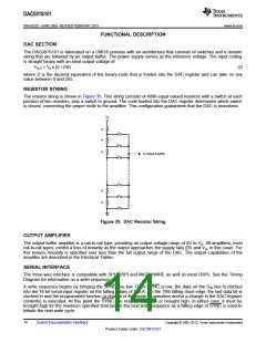
RESISTOR STRING
The resistor string is shown in Figure 35. This string consists of 4096 equal valued resistors with a switch at each
junction of two resistors, plus a switch to ground. The code loaded into the DAC register determines which switch
is closed, connecting the proper node to the amplifier. This configuration guarantees that the DAC is monotonic.
V
A
R
R
R
To Output Amplifier
R
R
Figure 35. DAC Resistor String
OUTPUT AMPLIFIER
The output buffer amplifier is a rail-to-rail type, providing an output voltage range of 0V to VA. All amplifiers, even
rail-to-rail types, exhibit a loss of linearity as the output approaches the supply rails (0V and VA, in this case). For
this reason, linearity is specified over less than the full output range of the DAC. The output capabilities of the
amplifier are described in the Electrical Tables.
SERIAL INTERFACE
The three-wire interface is compatible with SPI, QSPI and MICROWIRE as well as most DSPs. See the Timing
Diagram for information on a write sequence.
A write sequence begins by bringing the SYNC line low. Once SYNC is low, the data on the DIN line is clocked
into the 16-bit serial input register on the falling edges of SCLK. On the 16th falling clock edge, the last data bit is
clocked in and the programmed function (a change in the mode of operation and/or a change in the DAC register
contents) is executed. At this point the SYNC line may be kept low or brought high. In either case, it must be
brought high for the minimum specified time before the next write sequence as a falling edge of SYNC is used to
initiate the next write cycle.
14
Submit Documentation Feedback
Copyright © 2005–2013, Texas Instruments Incorporated
Product Folder Links: DAC081S101

 TI [ TEXAS INSTRUMENTS ]