DAC081S101
www.ti.com
SNAS323C –JUNE 2005–REVISED FEBRUARY 2013
Since the SYNC and DIN buffers draw more current when they are high, they should be idled low between write
sequences to minimize power consumption.
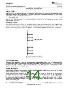
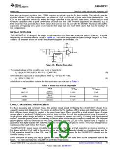
INPUT SHIFT REGISTER
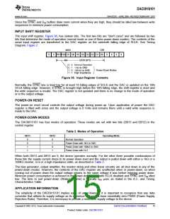
The input shift register, Figure 36, has sixteen bits. The first two bits are "don't cares" and are followed by two
bits that determine the mode of operation (normal mode or one of three power-down modes). The contents of the
serial input register are transferred to the DAC register on the sixteenth falling edge of SCLK. See Timing
Diagram, Figure 2.
MSB
LSB
X
X
PD1PD0 D7 D6 D5 D4 D3 D2 D1 D0
DATA BITS
X
X
X
X
0
0
1
1
0
1
0
1
Normal Operation
1 kW to GND
Power-Down Modes
100 kW to GND
High Impedance
Figure 36. Input Register Contents
Normally, the SYNC line is kept low for at least 16 falling edges of SCLK and the DAC is updated on the 16th
SCLK falling edge. However, if SYNC is brought high before the 16th falling edge, the shift register is reset and
the write sequence is invalid. The DAC register is not updated and there is no change in the mode of operation
or in the output voltage.
POWER-ON RESET
The power-on reset circuit controls the output voltage during power-up. Upon application of power the DAC
register is filled with zeros and the output voltage is 0 Volts and remains there until a valid write sequence is
made to the DAC.
POWER-DOWN MODES
The DAC081S101 has four modes of operation. These modes are set with two bits (DB13 and DB12) in the
control register.
Table 2. Modes of Operation
DB13
DB12
Operating Mode
0
0
1
1
0
1
0
1
Normal Operation
Power-Down with 1kΩ to GND
Power-Down with 100kΩ to GND
Power-Down with Hi-Z
When both DB13 and DB12 are 0, the device operates normally. For the other three possible combinations of
these bits the supply current drops to its power-down level and the output is pulled down with either a 1kΩ or a
100KΩ resistor, or is in a high impedance state, as described in Table 2.
The bias generator, output amplifier, the resistor string and other linear circuitry are all shut down in any of the
power-down modes. However, the contents of the DAC register are unaffected when in power-down, so when
coming out of power down the output voltage returns to the same voltage it was before entering power down.
Minimum power consumption is achieved in the power-down mode with SCLK disabled and SYNC and DIN idled
low. The time to exit power-down (Wake-Up Time) is typically tWU µsec as stated in the A.C. and Timing
Characteristics Table.
APPLICATION INFORMATION
The simplicity of the DAC081S101 implies ease of use. However, it is important to recognize that any data
converter that utilizes its supply voltage as its reference voltage will have essentially zero PSRR (Power Supply
Rejection Ratio). Therefore, it is necessary to provide a noise-free supply voltage to the device.
Copyright © 2005–2013, Texas Instruments Incorporated
Submit Documentation Feedback
15
Product Folder Links: DAC081S101

 TI [ TEXAS INSTRUMENTS ]