the bootstrap diode, which is typically around 4nC. ΔV is the
maximum allowable voltage drop across the bypass capaci-
tor. A 0.1uF or larger value, good quality, ceramic capacitor
is recommended. The bypass capacitor should be placed as
close to the pins of the IC as possible to minimize the parasitic
inductance.
Detailed Operating Description
The LM5113 is designed to drive both the high-side and the
low-side enhancement mode Gallium Nitride FETs in a syn-
chronous buck or a half-bridge configuration. The outputs of
the LM5113 are independently controlled with TTL input
thresholds. The inputs of the LM5113 can withstand voltages
up to 14V regardless of the VDD voltage, and can be directly
connected to the outputs of PWM controllers.
Bootstrap Capacitor
The bootstrap capacitor provides the gate charge for the high-
side switch, dc bias power for HB under-voltage lockout cir-
cuit, and the reverse recovery charge of the bootstrap diode.
The required bypass capacitance can be calculated as fol-
lows:
The high side driver uses the floating bootstrap capacitor volt-
age to drive the high-side FET. As shown in Figure 1, the
bootstrap capacitor is recharged through an internal boot-
strap diode each cycle when the HS pin is pulled below the
VDD voltage. For inductive load applications the HS node will
fall to a negative potential, clamped by the low side FET.
Due to the intrinsic feature of enhancement mode GaN FETs
the source-to-drain voltage, when the gate is pulled low, is
usually higher than a diode forward voltage drop. This can
lead to an excessive bootstrap voltage that can damage the
high-side GaN FET. The LM5113 solves this problem with an
internal clamping circuit that prevents the bootstrap voltage
from exceeding 5.2V typical.
IHB is the quiescent current of the high-side driver. ton is the
maximum on-time period of the high-side transistor. A good
quality, ceramic capacitor should be used for the bootstrap
capacitor. It is recommended to place the bootstrap capacitor
as close to the HB and HS pins as possible.
The output pull-down and pull-up resistance of LM5113 is op-
timized for enhancement mode GaN FETs to achieve high
frequency, efficient operation. The 0.6Ω pull-down resistance
provides a robust low impedance turn-off path necessary to
eliminate undesired turn-on induced by high dv/dt or high di/
dt. The 2.1Ω pull-up resistance helps reduce the ringing and
over-shoot of the switch node voltage. The split outputs of the
LM5113 offer flexibility to adjust the turn-on and turn-off speed
by independently adding additional impedance in either the
turn-on path and/or the turn-off path.
Power Dissipation
The power consumption of the driver is an important measure
that determines the maximum achievable operating frequen-
cy of the driver. It should be kept below the maximum power
dissipation limit of the package at the operating temperature.
The total power dissipation of the LM5113 is the sum of the
gate driver losses and the bootstrap diode power loss.
The gate driver losses are incurred by charge and discharge
of the capacitive load. It can be approximated as
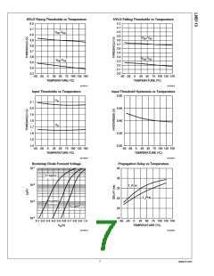
The LM5113 has an Under-voltage Lockout (UVLO) on both
the VDD and bootstrap supplies. When the VDD voltage is
below the threshold voltage of 3.8V, both the HI and LI inputs
are ignored, to prevent the GaN FETs from being partially
turned on. Also if there is sufficient VDD voltage, the UVLO
will actively pull the LOL and HOL low. When the HB to HS
bootstrap voltage is below the UVLO threshold of 3.2V, only
HOL is pulled low. Both UVLO threshold voltages have
200mV of hysteresis to avoid chattering.
CLoadH and CLoadL are the high-side and the low-side capaci-
tive loads respectively. It can also be calculated with the total
input gate charge of the high-side and the low-side transistors
as
Bypass Capacitor
The VDD bypass capacitor provides the gate charge for the
low-side and high-side transistors and to absorb the reverse
recovery charge of the bootstrap diode. The required bypass
capacitance can be calculated as follows:
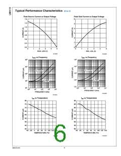
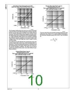
There are some additional losses in the gate drivers due to
the internal CMOS stages used to buffer the LO and HO out-
puts. The following plot shows the measured gate driver
power dissipation versus frequency and load capacitance. At
higher frequencies and load capacitance values, the power
dissipation is dominated by the power losses driving the out-
put loads and agrees well with the above equations. This plot
can be used to approximate the power losses due to the gate
drivers.
QgH and QgL are gate charge of the high-side and low-side
transistors respectively. Qrr is the reverse recovery charge of
9
www.ti.com

 TI [ TEXAS INSTRUMENTS ]