respective source of the high-side and low-side
transistors with a short and low-inductance path.
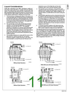
Layout Considerations
Small gate capacitance and miller capacitance enable en-
hancement mode GaN FETs to operate with fast switching
speed. The induced high dv/dt and di/dt, coupled with a low
gate threshold voltage and limited headroom of enhancement
mode GaN FETs gate voltage, make the circuit layout crucial
to the optimum performance. Following are some hints.
4. The parasitic source inductance, along with the gate
capacitor and the driver pull-down path, can form a LCR
resonant tank, resulting in gate voltage oscillations. An
optional resistor or ferrite bead can be used to damp the
ringing.
5. Low ESR/ESL capacitors must be connected close to the
IC, between VDD and VSS pins and between the HB and
HS pins to support the high peak current being drawn
from VDD during turn-on of the FETs. It is most desirable
to place the VDD decoupling capacitor and the HB to HS
bootstrap capacitor on the same side of the PC board as
the driver. The inductance of vias can impose excessive
ringing on the IC pins.
1. The first priority in designing the layout of the driver is to
confine the high peak currents that charge and discharge
the GaN FETs gate into a minimal physical area. This will
decrease the loop inductance and minimize noise issues
on the gate terminal of the GaN FETs. The GaN FETs
should be placed close to the driver.
2. The second high current path includes the bootstrap
capacitor, the local ground referenced VDD bypass
capacitor and low-side GaN FET. The bootstrap
capacitor is recharged on a cycle-by-cycle basis through
the bootstrap diode from the ground referenced VDD
capacitor. The recharging occurs in a short time interval
and involves high peak current. Minimizing this loop
length and area on the circuit board is important to ensure
reliable operation.
6. To prevent excessive ringing on the input power bus,
good decoupling practices are required by placing low
ESR ceramic capacitors adjacent to the GaN FETs.
The following figures show recommended layout patterns for
LLP-10 package and micro SMD package respectively. Two
cases are considered: (1) Without any gate resistors; (2) With
an optional turn-on gate resistor. It should be noted that 0402
SMD package is assumed for the passive components in the
drawings. For information on micro SMD package assembly,
refer to Application Note AN-1112.
3. The parasitic inductance in series with the source of the
high-side FET and the low-side FET can impose
excessive negative voltage transients on the driver. It is
recommended to connect HS pin and VSS pin to the
30162921
Without Gate Resistors
30162922
With HOH and LOH Gate Resistors
30162924
30162923
With HOH and LOH Gate Resistors
Without Gate Resistors
11
www.ti.com

 TI [ TEXAS INSTRUMENTS ]