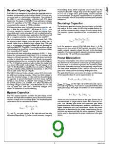
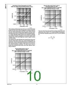
Gate Driver Power Dissipation (LO+HO)
VDD=+5V, Neglecting Bootstrap Diode Losses
Reverse Recovery Power Loss of
Bootstrap Diode VIN=50V
The Load of High-Side Driver is a GaN FET
with Total Gate Charge of 10nC
30162919
The bootstrap diode power loss is the sum of the forward bias
power loss that occurs while charging the bootstrap capacitor
and the reverse bias power loss that occurs during reverse
recovery. Since each of these events happens once per cycle,
the diode power loss is proportional to the operating frequen-
cy. Larger capacitive loads require more energy to recharge
the bootstrap capacitor resulting in more losses. Higher input
voltages (VIN) to the half bridge also result in higher reverse
recovery losses.
30162944
The sum of the driver loss and the bootstrap diode loss is the
total power loss of the IC. For a given ambient temperature,
the maximum allowable power loss of the IC can be defined
as
The following two plots illustrate the forward bias power loss
and the reverse bias power loss of the bootstrap diode re-
spectively. The plots are generated based on calculations and
lab measurements of the diode reverse time and current un-
der several operating conditions. The plots can be used to
predict the bootstrap diode power loss under different oper-
ating conditions.
Forward Bias Power Loss of
Bootstrap Diode VIN=50V
The Load of High-Side Driver is a GaN FET
with Total Gate Charge of 10nC
30162943
www.ti.com
10

 TI [ TEXAS INSTRUMENTS ]