Switching Characteristics
Limits in standard type are for TJ = 25°C only; limits in boldface type apply over the junction temperature (TJ) range of -40°C to
+125°C. Minimum and Maximum limits are guaranteed through test, design, or statistical correlation. Typical values represent the
most likely parametric norm at TJ = 25°C, and are provided for reference purposes only. Unless otherwise specified, VDD = VHB
=
5V, VSS = VHS = 0V, No Load on LOL and LOH or HOL and HOH (Note 3).
Symbol
tLPHL
Parameter
Conditions
Min
Typ
26.5
28.0
26.5
28.0
1.5
Max
45.0
45.0
45.0
45.0
8.0
Units
LO Turn-Off Propagation Delay
LO Turn-On Propagation Delay
HO Turn-Off Propagation Delay
HO Turn-On Propagation Delay
Delay Matching: LO on & HO off
Delay Matching: LO off & HO on
HO Rise Time (0.5V - 4.5V)
LO Rise Time (0.5V – 4.5V)
HO Fall Time (0.5V - 4.5V)
LI Falling to LOL Falling
LI Rising to LOH Rising
HI Falling to HOL Falling
HI Rising to HOH Rising
ns
ns
ns
ns
ns
ns
ns
ns
ns
ns
tLPLH
tHPHL
tHPLH
tMON
tMOFF
tHRC
tLRC
1.5
8.0
CL = 1000 pF
CL = 1000 pF
CL = 1000 pF
CL = 1000 pF
7.0
7.0
tHFC
tLFC
1.5
LO Fall Time (0.5V - 4.5V)
1.5
tPW
Minimum Input Pulse Width that Changes
the Output
10
40
ns
ns
tBS
Bootstrap Diode Reverse Recovery Time IF = 100mA,
IR = 100mA
Note 2: Absolute Maximum Ratings indicate limits beyond which damage to the component may occur. Operating Ratings are conditions under which operation
of the device is guaranteed. Operating Ratings do not imply guaranteed performance limits. For guaranteed performance limits and associated test conditions,
see the Electrical Characteristics tables.
Note 3: Min and Max limits are 100% production tested at 25°C. Limits over the operating temperature range are guaranteed through correlation using Statistical
Quality Control (SQC) methods. Limits are used to calculate National’s Average Outgoing Quality Level (AOQL).
Note 4: Four layer board with Cu finished thickness 1.5/1/1/1.5 oz. Maximum die size used. 5x body length of Cu trace on PCB top. 50 x 50mm ground and power
planes embedded in PCB. See Application Note AN-1187.
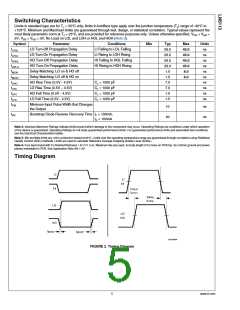
Timing Diagram
30162904
FIGURE 2. Timing Diagram
5
www.ti.com

 TI [ TEXAS INSTRUMENTS ]