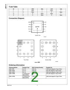
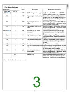
Pin Descriptions
Pin Number
Name
Description
Applications Information
micro SMD
LLP-10
A3, C4 (Note 1)
1
VDD
HB
5V Positive gate drive supply
Locally decouple to VSS using low ESR/ESL
capacitor located as close to the IC as possible.
D3
2
High-side gate driver bootstrap Connect the positive terminal of the bootstrap
rail
capacitor to HB and the negative terminal to HS.
The bootstrap capacitor should be placed as
close to the IC as possible.
D2
3
4
5
6
7
HOH
HOL
HS
HI
High-side gate driver turn-on
output
Connect to the gate of high-side GaN FET with a
short, low inductance path. A gate resistor can be
used to adjust the turn-on speed.
D1
High-side gate driver turn-off
output
Connect to the gate of high-side GaN FET with a
short, low inductance path. A gate resistor can be
used to adjust the turn-off speed.
C1, D4 (Note 1)
High-side GaN FET source
connection
Connect to the bootstrap capacitor negative
terminal and the source of the high-side GaN
FET.
B4
A4
High-side driver control input
Low-side driver control input
Ground return
The LM5113 inputs have TTL type thresholds.
Unused inputs should be tied to ground and not
left open.
LI
The LM5113 inputs have TTL type thresholds.
Unused inputs should be tied to ground and not
left open.
A2
A1
8
9
VSS
LOL
All signals are referenced to this ground.
Low-side gate driver sink-current Connect to the gate of the low-side GaN FET with
output
a short, low inductance path. A gate resistor can
be used to adjust the turn-off speed.
B1
10
LOH
Low-side gate driver source-
current output
Connect to the gate of high-side GaN FET with a
short, low inductance path. A gate resistor can be
used to adjust the turn-on speed.
EP
Exposed Pad
It is recommended that the exposed pad on the
bottom of the package be soldered to ground
plane on the PC board to aid thermal dissipation.
Note 1: A3 and C4, C1 and D4 are internally connected.
3
www.ti.com

 TI [ TEXAS INSTRUMENTS ]