LM3886
www.ti.com
SNAS091C –MAY 1999–REVISED MARCH 2013
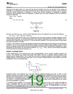
The desired input impedance is set by RIN. Very high values can cause board layout problems and DC offsets at
the output. The value for the feedback resistance, Rf1, should be chosen to be a relatively large value (10
kΩ–100 kΩ), and the other feedback resistance, Ri, is calculated using standard op amp configuration gain
equations. Most audio amplifiers are designed from the non-inverting amplifier configuration.
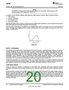
DESIGN A 40W/4Ω AUDIO AMPLIFIER
Given:
Power Output
Load Impedance
Input Level
40W
4Ω
1V(max)
Input Impedance
Bandwidth
100 kΩ
20 Hz–20 kHz ± 0.25 dB
Equation 7 and Equation 8 give:
40W/4Ω
Vopeak = 17.9V
Iopeak = 4.5A
Therefore the supply required is: ±21.0V at 4.5A
With 15% regulation and high line the final supply voltage is ±26.6V using Equation 9. At this point it is a good
idea to check the Power Output vs Supply Voltage to ensure that the required output power is obtainable from
the device while maintaining low THD + N. It is also good to check the Power Dissipation vs Supply Voltage to
ensure that the device can handle the internal power dissipation. At the same time designing in a relatively
practical sized heat sink with a low thermal resistance is also important. Refer to Typical Performance
Characteristics graphs and THERMAL CONSIDERATIONS for more information.
The minimum gain from Equation 10 is: AV ≥ 12.6
We select a gain of 13 (Non-Inverting Amplifier); resulting in a sensitivity of 973 mV.
Letting RIN equal 100 kΩ gives the required input impedance, however, this would eliminate the “volume control”
unless an additional input impedance was placed in series with the 10 kΩ potentiometer that is depicted in
Figure 1. Adding the additional 100 kΩ resistor would ensure the minumum required input impedance.
For low DC offsets at the output we let Rf1 = 100 kΩ. Solving for Ri (Non-Inverting Amplifier) gives the following:
Ri = Rf1/(AV − 1) = 100k/(13 − 1) = 8.3 kΩ; use 8.2 kΩ
The bandwidth requirement must be stated as a pole, i.e., the 3 dB frequency. Five times away from a pole gives
0.17 dB down, which is better than the required 0.25 dB. Therefore:
fL = 20 Hz/5 = 4 Hz
(11)
(12)
fH = 20 kHz × 5 = 100 kHz
At this point, it is a good idea to ensure that the Gain-Bandwidth Product for the part will provide the designed
gain out to the upper 3 dB point of 100 kHz. This is why the minimum GBWP of the LM3886 is important.
GBWP ≥ AV × f3 dB = 13 × 100 kHz = 1.3 MHz
(13)
(14)
GBWP = 2.0 MHz (min) for the LM3886
Solving for the low frequency roll-off capacitor, Ci, we have:
Ci ≥ 1/(2π Ri fL) = 4.85 μF; use 4.7 μF.
(15)
Definition of Terms
Input Offset Voltage: The absolute value of the voltage which must be applied between the input terminals
through two equal resistances to obtain zero output voltage and current.
Input Bias Current: The absolute value of the average of the two input currents with the output voltage and
current at zero.
Input Offset Current:The absolute value of the difference in the two input currents with the output voltage and
current at zero.
Input Common-Mode Voltage Range (or Input Voltage Range): The range of voltages on the input terminals
Copyright © 1999–2013, Texas Instruments Incorporated
Submit Documentation Feedback
23
Product Folder Links: LM3886

 TI [ TEXAS INSTRUMENTS ]