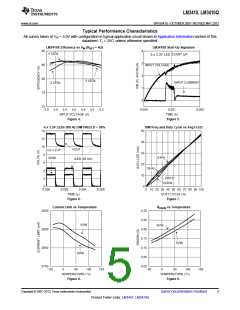
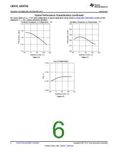
LM3410, LM3410Q
SNVS541G –OCTOBER 2007–REVISED MAY 2013
www.ti.com
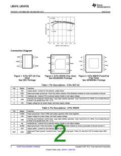
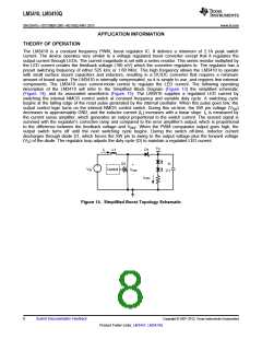
Connection Diagram
SW
1
5
4
VIN
DIM
PGND
VIN
SW
NC
PGND
VIN
1
2
3
4
8
7
6
5
NC
1
2
6
5
SW
GND
2
3
AGND
AGND
FB
FB
DIM
DIM
FB
3
4
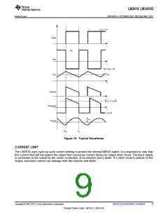
Figure 1. 5-Pin SOT-23 (Top
View)
Figure 2. 6-Pin WSON (Top View) Figure 3. 8-Pin MSOP-PowerPad
(Top View)
See NGG0006A Package
See DBV Package
See GDN0008A Package
Table 1. Pin Descriptions - 5-Pin SOT-23
Pin
1
Name
SW
Function
Output switch. Connect to the inductor, output diode.
2
GND
FB
Signal and power ground pin. Place the bottom resistor of the feedback network as close as possible to this pin.
Feedback pin. Connect FB to external resistor divider to set output voltage.
3
Dimming and shutdown control input. Logic high enables operation. Duty Cycle from 0 to 100%. Do not allow this pin
to float or be greater than VIN + 0.3V.
4
5
DIM
VIN
Supply voltage pin for power stage, and input supply voltage.
Table 2. Pin Descriptions - 6-Pin WSON
Pin
1
Name
PGND
VIN
Function
Power ground pin. Place PGND and output capacitor GND close together.
Supply voltage for power stage, and input supply voltage.
2
Dimming and shutdown control input. Logic high enables operation. Duty Cycle from 0 to 100%. Do not allow this pin
to float or be greater than VIN + 0.3V.
3
DIM
4
5
6
FB
AGND
SW
Feedback pin. Connect FB to external resistor divider to set output voltage.
Signal ground pin. Place the bottom resistor of the feedback network as close as possible to this pin and pin 4.
Output switch. Connect to the inductor, output diode.
Signal and Power ground. Connect to pin 1 and pin 5 on top layer. Place 4-6 vias from DAP to bottom layer GND
plane.
DAP
GND
2
Submit Documentation Feedback
Copyright © 2007–2013, Texas Instruments Incorporated
Product Folder Links: LM3410 LM3410Q

 TI [ TEXAS INSTRUMENTS ]