LM27761
ZHCSEO7C –OCTOBER 2015–REVISED JANUARY 2017
www.ti.com.cn
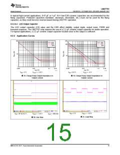
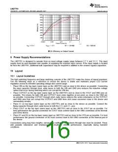
100%
90%
80%
70%
60%
50%
40%
30%
20%
10%
25°C
85°C
-40°C
0
0.0001
0.001
0.01
0.1
1
Output Current (A)
D005
VIN = 5.5 V
VOUT = –5 V
R1 = 1.54 MΩ
R2 = 500 kΩ
图 22. Efficiency vs Output Current
9 Power Supply Recommendations
The LM27761 is designed to operate from an input voltage supply range between 2.7 V and 5.5 V. This input
supply must be well regulated and capable of supplying the required input current. If the input supply is located
far form the LM27761, additional bulk capacitance may be required in addition to the ceramic bypass capacitors.
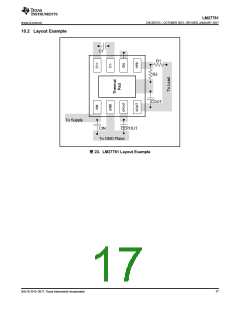
10 Layout
10.1 Layout Guidelines
The high switching frequency and large switching currents of the LM27761 make the choice of layout important.
Use the following steps as a reference to ensure the device is stable and maintains proper LED current
regulation across its intended operating voltage and current range:
•
Place CIN on the top layer (same layer as the LM27761) and as close to the device as possible. Connecting
the input capacitor through short, wide traces to both the VIN and GND pins reduces the inductive voltage
spikes that occur during switching which can corrupt the VIN line.
•
Place CCPOUT on the top layer (same layer as the LM27761) and as close to the VOUT and GND pins as
possible. The returns for both CIN and CCPOUT must come together at one point, as close to the GND pin
as possible. Connecting CCPOUT through short, wide traces reduces the series inductance on the VCPOUT
and GND pins that can corrupt the VCPOUT and GND lines and cause excessive noise in the device and
surrounding circuitry.
•
•
Place C1 on top layer (same layer as the LM27761) and as close to the device as possible. Connect the
flying capacitor through short, wide traces to both the C1+ and C1– pins.
Place COUT on the top layer (same layer as the LM27761) and as close to the VOUT pin as possible. For
best performance the ground connection for COUT must connect back to the GND connection at the thermal
pad of the device.
•
Place R1 and R2 on the top layer (same layer as LM27761) and as close to the VFB pin as possible. For best
performance the ground connection of R2 must connect back to the GND connection at the thermal pad of
the device.
Connections using long trace lengths, narrow trace widths, or connections through vias must be avoided. These
add parasitic inductance and resistance that results in inferior performance, especially during transient
conditions.
16
版权 © 2015–2017, Texas Instruments Incorporated

 TI [ TEXAS INSTRUMENTS ]