LM27761
ZHCSEO7C –OCTOBER 2015–REVISED JANUARY 2017
www.ti.com.cn
8.2.2 Detailed Design Procedure
8.2.2.1 Custom Design With WEBENCH® Tools
Click here to create a custom design using the LM27761 device with the WEBENCH® Power Designer.
1. Start by entering the input voltage (VIN), output voltage (VOUT), and output current (IOUT) requirements.
2. Optimize the design for key parameters such as efficiency, footprint, and cost using the optimizer dial.
3. Compare the generated design with other possible solutions from Texas Instruments.
The WEBENCH Power Designer provides a customized schematic along with a list of materials with real-time
pricing and component availability.
In most cases, these actions are available:
•
•
•
•
Run electrical simulations to see important waveforms and circuit performance
Run thermal simulations to understand board thermal performance
Export customized schematic and layout into popular CAD formats
Print PDF reports for the design, and share the design with colleagues
Get more information about WEBENCH tools at www.ti.com/WEBENCH.
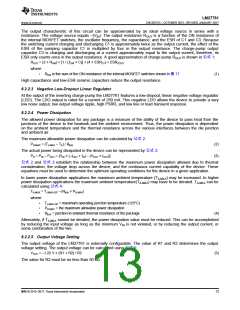
8.2.2.2 Charge-Pump Voltage Inverter
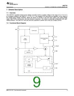
The main application of the LM27761 is to generate a regulated negative supply voltage. The voltage inverter
circuit uses only three external capacitors, and the LDO regulator circuit uses one additional output capacitor.
The voltage inverter portion of the LM27761 contains four large CMOS switches which are switched in sequence
to invert the input supply voltage. Energy transfer and storage are provided by external capacitors. 图 17 shows
the voltage switches S2 and S4 are open. In the second time interval, S1 and S3 are open; at the same time, S2
and S4 are closed, and C1 is charging C3. After a number of cycles, the voltage across C3 is pumped into VIN.
Because the anode of C3 is connected to ground, the output at the cathode of C3 equals –(VIN) when there is no
load current. When a load is added the output voltage dropis determined by the parasitic resistance (RDSON of the
MOSFET switches and the equivalent series resistance (ESR) of the capacitors) and the charge transfer loss
between the capacitors.
S1
C1+
S2
VIN
CIN
GND
C1
COUT
GND
S3
S4
C1-
CPOUT
OSC.
2 MHz
+
PFM COMP
VIN
图 17. Voltage Inverting Principle
12
版权 © 2015–2017, Texas Instruments Incorporated

 TI [ TEXAS INSTRUMENTS ]