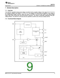
LM27761
www.ti.com.cn
ZHCSEO7C –OCTOBER 2015–REVISED JANUARY 2017
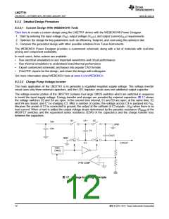
The output characteristic of this circuit can be approximated by an ideal voltage source in series with a
resistance. The voltage source equals –(VIN). The output resistance ROUT is a function of the ON resistance of
the internal MOSFET switches, the oscillator frequency, the capacitance, and the ESR of C1 and C3. Because
the switching current charging and discharging C1 is approximately twice as the output current, the effect of the
ESR of the pumping capacitor C1 is multiplied by four in the output resistance. The charge-pump output
capacitor C3 is charging and discharging at a current approximately equal to the output current; therefore, its
ESR only counts once in the output resistance. A good approximation of charge-pump ROUT is shown in 公式 1:
ROUT = (2 × RSW) + [1 / (ƒSW × C)] + (4 × ESRC1) + ESRCOUT
where
•
RSW is the sum of the ON resistance of the internal MOSFET switches shown in 图 17.
(1)
High capacitance and low-ESR ceramic capacitors reduce the output resistance.
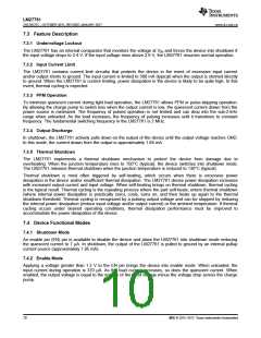
8.2.2.3 Negative Low-Dropout Linear Regulator
At the output of the inverting charge-pump the LM27761 features a low-dropout, linear negative voltage regulator
(LDO). The LDO output is rated for a current of 250 mA. This negative LDO allows the device to provide a very
low noise output, low output voltage ripple, high PSRR, and low line or load transient response.
8.2.2.4 Power Dissipation
The allowed power dissipation for any package is a measure of the ability of the device to pass heat from the
junctions of the device to the heatsink and the ambient environment. Thus, the power dissipation is dependent
on the ambient temperature and the thermal resistance across the various interfaces between the die junction
and ambient air.
The maximum allowable power dissipation can be calculated by 公式 2:
PD-MAX = (TJ-MAX – TA) / RθJA
(2)
The actual power being dissipated in the device can be represented by 公式 3:
PD = PIN – POUT = [VIN × (–IOUT + IQ) – (VOUT × IOUT)]
(3)
公式 2 and 公式 3 establish the relationship between the maximum power dissipation allowed due to thermal
consideration, the voltage drop across the device, and the continuous current capability of the device. These
equations must be used to determine the optimum operating conditions for the device in a given application.
In lower power dissipation applications the maximum ambient temperature (TA-MAX) may be increased. In higher
power dissipation applications the maximum ambient temperature(TA-MAX) may have to be derated. TA-MAX can be
calculated using 公式 4:
TA-MAX = TJ-MAX-OP – (RθJA × PD-MAX
)
where
•
•
•
TJ-MAX-OP = maximum operating junction temperature (125°C)
PD-MAX = the maximum allowable power dissipation
RθJA = junction-to-ambient thermal resistance of the package
(4)
Alternately, if TA-MAX cannot be derated, the power dissipation value must be reduced. This can be accomplished
by reducing the input voltage as long as the minimum VIN is not violated, or by reducing the output current, or
some combination of the two.
8.2.2.5 Output Voltage Setting
The output voltage of the LM27761 is externally configurable. The value of R1 and R2 determines the output
voltage setting. The output voltage can be calculated using 公式 5:
VOUT = –1.22 V × (R1 + R2) / R2
(5)
The value for R2 must be no less than 50 kΩ.
版权 © 2015–2017, Texas Instruments Incorporated
13

 TI [ TEXAS INSTRUMENTS ]