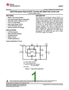
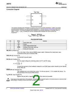
LM2703
www.ti.com
SNVS172F –FEBRUARY 2002–REVISED MAY 2013
(1)(2)
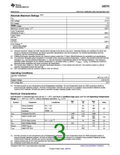
Absolute Maximum Ratings
VIN
7.5V
22.5V
2V
SW Voltage
FB Voltage
SHDN Voltage
7.5V
(3)
Maximum Junction Temp. TJ
150°C
Lead Temperature
(Soldering 10 sec.)
300°C
215°C
220°C
Vapor Phase
(60 sec.)
Infrared
(15 sec.)
(4)
ESD Ratings
Human Body Model
Machine Model
2kV
200V
(5)
(1) Absolute maximum ratings are limits beyond which damage to the device may occur. Operating Ratings are conditions for which the
device is intended to be functional, but device parameter specifications may not be ensured. For ensured specifications and test
conditions, see the Electrical Characteristics.
(2) If Military/Aerospace specified devices are required, please contact the TI Sales Office/Distributors for availability and specifications.
(3) The maximum allowable power dissipation is a function of the maximum junction temperature, TJ(MAX), the junction-to-ambient thermal
resistance, θJA, and the ambient temperature, TA. See the Electrical Characteristics table for the thermal resistance. The maximum
allowable power dissipation at any ambient temperature is calculated using: PD (MAX) = (TJ(MAX) − TA)/θJA. Exceeding the maximum
allowable power dissipation will cause excessive die temperature.
(4) The human body model is a 100 pF capacitor discharged through a 1.5 kΩ resistor into each pin. The machine model is a 200 pF
capacitor discharged directly into each pin.
(5) ESD susceptibility using the machine model is 150V for SW pin.
Operating Conditions
Junction Temperature
(1)
−40°C to +125°C
Supply Voltage
2.2V to 7V
22V
SW Voltage Max.
(1) All limits ensured at room temperature and at temperature extremes. All room temperature limits are 100% production tested or
ensured through statistical analysis. All limits at temperature extremes are ensured via correlation using standard Statistical Quality
Control (SQC) methods. All limits are used to calculate Average Outgoing Quality Level (AOQL).
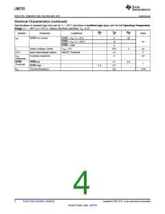
Electrical Characteristics
Specifications in standard type face are for TJ = 25°C and those in boldface type apply over the full Operating Temperature
Range (TJ = −40°C to +125°C). Unless otherwise specified. VIN =2.2V.
Min
Typ
Max
Symbol
Parameter
Conditions
Units
(1)
(2)
(1)
IQ
Device Disabled
FB = 1.3V
FB = 1.2V
40
235
70
300
Device Enabled
Shutdown
µA
SHDN = 0V
0.01
1.237
350
2.5
VFB
ICL
FeedbackTrip Point
Switch Current Limit
1.189
1.269
V
275
400
mA
260
400
(3)
IB
FB Pin Bias Current
Input Voltage Range
Switch RDSON
FB = 1.23V
30
120
7.0
1.6
nA
V
VIN
2.2
RDSON
TOFF
0.7
Ω
Switch Off Time
400
ns
(1) All limits ensured at room temperature and at temperature extremes. All room temperature limits are 100% production tested or
ensured through statistical analysis. All limits at temperature extremes are ensured via correlation using standard Statistical Quality
Control (SQC) methods. All limits are used to calculate Average Outgoing Quality Level (AOQL).
(2) Typical numbers are at 25°C and represent the most likely norm.
(3) Feedback current flows into the pin.
Copyright © 2002–2013, Texas Instruments Incorporated
Submit Documentation Feedback
3
Product Folder Links: LM2703

 TI [ TEXAS INSTRUMENTS ]