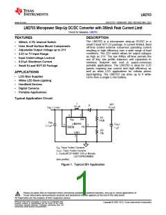
LM2703
SNVS172F –FEBRUARY 2002–REVISED MAY 2013
www.ti.com
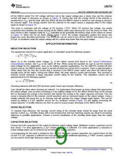
Connection Diagram
Top View
VIN
SW
GND
SHDN
FB
The maximum allowable power dissipation is a function of the maximum junction temperature, TJ(MAX), the junction-
to-ambient thermal resistance, θJA, and the ambient temperature, TA. See the Electrical Characteristics table for the
thermal resistance. The maximum allowable power dissipation at any ambient temperature is calculated using: PD
(MAX) = (TJ(MAX) − TA)/θJA. Exceeding the maximum allowable power dissipation will cause excessive die
temperature.
Figure 2. SOT23-5
TJmax = 125°C, θJA = 220°C/W
PIN DESCRIPTIONS
Pin
1
Name
SW
Function
Power Switch input.
2
GND
FB
Ground.
3
Output voltage feedback input.
Shutdown control input, active low.
Analog and Power input.
4
SHDN
VIN
5
SW (Pin 1):Switch Pin.
This is the drain of the internal NMOS power switch. Minimize the metal trace area
connected to this pin to minimize EMI.
GND (Pin 2):Ground Pin.
Tie directly to ground plane.
FB (Pin 3):Feedback Pin.
Set the output voltage by selecting values for R1 and R2 using:
(
VOUT
-1
R1 = R2
1.237V
(1)
Connect the ground of the feedback network to an AGND plane which should be tied directly
to the GND pin.
SHDN (Pin 4):Shutdown Pin.
The shutdown pin is an active low control. Tie this pin above 1.1V to enable the device. Tie
this pin below 0.3V to turn off the device.
VIN (Pin 5): Input Supply Pin.
Bypass this pin with a capacitor as close to the device as possible.
These devices have limited built-in ESD protection. The leads should be shorted together or the device placed in conductive foam
during storage or handling to prevent electrostatic damage to the MOS gates.
2
Submit Documentation Feedback
Copyright © 2002–2013, Texas Instruments Incorporated
Product Folder Links: LM2703

 TI [ TEXAS INSTRUMENTS ]