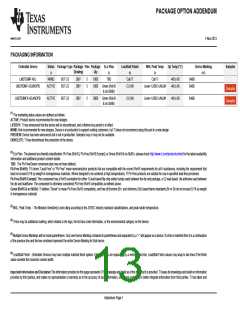
LM2703
www.ti.com
SNVS172F –FEBRUARY 2002–REVISED MAY 2013
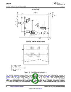
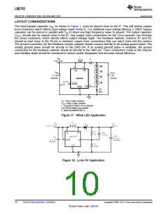
off the NMOS switch.The SW voltage will then rise to the output voltage plus a diode drop and the inductor
current will begin to decrease as shown in Figure 16. During this time the energy stored in the inductor is
transferred to COUT and the load. After the 400ns off-time the NMOS switch is turned on and energy is stored in
the inductor again. This energy transfer from the inductor to the output causes a stepping effect in the output
ripple as shown in Figure 16.
This cycle is continued until the voltage at FB reaches 1.237V. When FB reaches this voltage, the enable
comparator then disables the device turning off the NMOS switch and reducing the Iq of the device to 40uA. The
load current is then supplied solely by COUT indicated by the gradually decreasing slope at the output as shown
in Figure 16. When the FB pin drops slightly below 1.237V, the enable comparator enables the device and
begins the cycle described previously. The SHDN pin can be used to turn off the LM2703 and reduce the Iq to
0.01µA. In shutdown mode the output voltage will be a diode drop lower than the input voltage.
APPLICATION INFORMATION
INDUCTOR SELECTION
The appropriate inductor for a given application is calculated using the following equation:
(
VOUT - VIN(min) + VD
L =
TOFF
ICL
(2)
where VD is the schottky diode voltage, ICL is the switch current limit found in the Typical Performance
Characteristics section, and TOFF is the switch off time. When using this equation be sure to use the minimum
input voltage for the application, such as for battery powered applications. For the LM2703 constant-off time
control scheme, the NMOS power switch is turned off when the current limit is reached. There is approximately a
200ns delay from the time the current limit is reached in the NMOS power switch and when the internal logic
actually turns off the switch. During this 200ns delay, the peak inductor current will increase. This increase in
inductor current demands a larger saturation current rating for the inductor. This saturation current can be
approximated by the following equation:
(
VIN(max)
200ns
IPK = ICL
+
L
(3)
Choosing inductors with low ESR decrease power losses and increase efficiency.
Care should be taken when choosing an inductor. For applications that require an input voltage that approaches
the output voltage, such as when converting a Li-Ion battery voltage to 5V, the 400ns off time may not be enough
time to discharge the energy in the inductor and transfer the energy to the output capacitor and load. This can
cause a ramping effect in the inductor current waveform and an increased ripple on the output voltage. Using a
smaller inductor will cause the IPK to increase and will increase the output voltage ripple further. This can be
solved by adding a 4.7pF capacitor across the RF1 feedback resistor (Figure 15) and slightly increasing the
output capacitor. A smaller inductor can then be used to ensure proper discharge in the 400ns off time.
DIODE SELECTION
To maintain high efficiency, the average current rating of the schottky diode should be larger than the peak
inductor current, IPK. Schottky diodes with a low forward drop and fast switching speeds are ideal for increasing
efficiency in portable applications. Choose a reverse breakdown of the schottky diode larger than the output
voltage.
CAPACITOR SELECTION
Choose low ESR capacitors for the output to minimize output voltage ripple. Multilayer ceramic capacitors are the
best choice. For most applications, a 1µF ceramic capacitor is sufficient. For some applications a reduction in
output voltage ripple can be achieved by increasing the output capacitor.
Local bypassing for the input is needed on the LM2703. Multilayer ceramic capacitors are a good choice for this
as well. A 4.7µF capacitor is sufficient for most applications. For additional bypassing, a 100nF ceramic capacitor
can be used to shunt high frequency ripple on the input.
Copyright © 2002–2013, Texas Instruments Incorporated
Submit Documentation Feedback
9
Product Folder Links: LM2703

 TI [ TEXAS INSTRUMENTS ]