LM2703
SNVS172F –FEBRUARY 2002–REVISED MAY 2013
www.ti.com
OPERATION
L
D
V
V
IN
OUT
C
V
IN
SW
IN
5
1
C
OUT
R1
R2
50k
50k
Enable
Comp
V
OUT
+
-
Enable
R
F1
FB
Q2
10x
Q1
3
+
R
CL
Comp
-
F2
R3
Current Sensing
Circuitry
30k
400ns
One Shot
Driver
CL Adjust
Logic
R4
140k
Under Voltage
Lockout
4
2
GND
SHDN
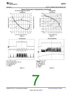
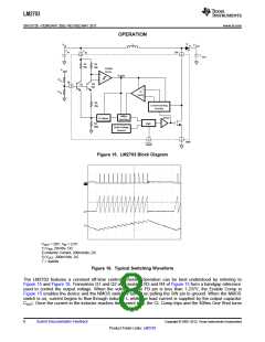
Figure 15. LM2703 Block Diagram
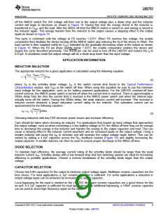
VOUT = 20V, VIN = 2.5V
1) VSW, 20V/div, DC
2) Inductor Current, 200mA/div, DC
3) VOUT, 200mV/div, AC
T = 4µs/div
Figure 16. Typical Switching Waveform
The LM2703 features a constant off-time control scheme. Operation can be best understood by referring to
Figure 15 and Figure 16. Transistors Q1 and Q2 and resistors R3 and R4 of Figure 15 form a bandgap reference
used to control the output voltage. When the voltage at the FB pin is less than 1.237V, the Enable Comp in
Figure 15 enables the device and the NMOS switch is turned on pulling the SW pin to ground. When the NMOS
switch is on, current begins to flow through inductor L while the load current is supplied by the output capacitor
COUT. Once the current in the inductor reaches the current limit, the CL Comp trips and the 400ns One Shot turns
8
Submit Documentation Feedback
Copyright © 2002–2013, Texas Instruments Incorporated
Product Folder Links: LM2703

 TI [ TEXAS INSTRUMENTS ]