LM26420, LM26420-Q0, LM26420-Q1
SNVS579J –FEBRUARY 2009–REVISED SEPTEMBER 2015
www.ti.com
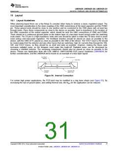
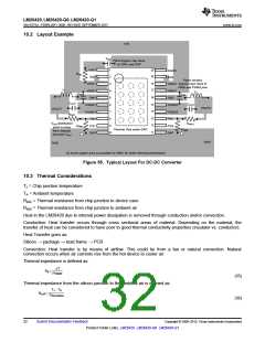
10.2 Layout Example
VIN
CINC
Place bypass cap close
to VINC and DAP
1
2
20
19
VINC
EN1
AGND
EN2
RINC
Place ceramic
VIND1
18
17
bypass caps close to
VIND and PGND pins
3
4
VIND2
VIND2
L1
VIND1
SW1
L2
CIN1
CIN2
16
15
14
13
12
11
5
SW2
COUT1
COUT2
PGND1
6
PGND2
VOUT2
VOUT1
7
PGND1
FB1
PGND2
FB2
RFBT1
8
VOUT distribution
point is away
from inductor
and past COUT
RFBT2
RFBB2
9
PG1
PG2
RFBB1
Thermal Vias under DAP
10
DAP
DAP
GND
GND
As much copper area as possible for GND, for better thermal performance
Figure 55. Typical Layout For DC-DC Converter
10.3 Thermal Considerations
TJ = Chip junction temperature
TA = Ambient temperature
R
θJC = Thermal resistance from chip junction to device case
θJA = Thermal resistance from chip junction to ambient air
R
Heat in the LM26420 due to internal power dissipation is removed through conduction and/or convection.
Conduction: Heat transfer occurs through cross sectional areas of material. Depending on the material, the
transfer of heat can be considered to have poor to good thermal conductivity properties (insulator vs. conductor).
Heat Transfer goes as:
Silicon → package → lead frame → PCB
Convection: Heat transfer is by means of airflow. This could be from a fan or natural convection. Natural
convection occurs when air currents rise from the hot device to cooler air.
Thermal impedance is defined as:
'T
RTꢀ=
Power
(35)
Thermal impedance from the silicon junction to the ambient air is defined as:
TJ - TA
RTJAꢀ
=
PINTERNAL
(36)
32
Submit Documentation Feedback
Copyright © 2009–2015, Texas Instruments Incorporated
Product Folder Links: LM26420 LM26420-Q0 LM26420-Q1

 TI [ TEXAS INSTRUMENTS ]