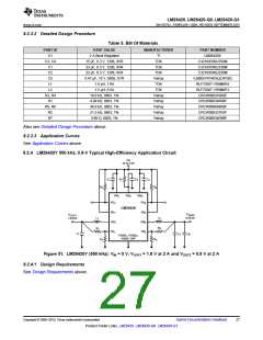
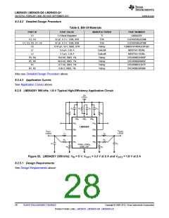
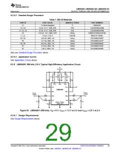
LM26420, LM26420-Q0, LM26420-Q1
www.ti.com
SNVS579J –FEBRUARY 2009–REVISED SEPTEMBER 2015
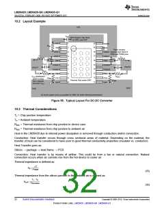
10 Layout
10.1 Layout Guidelines
When planning layout there are a few things to consider when trying to achieve a clean, regulated output. The
most important consideration is the close coupling of the GND connections of the input capacitor and the PGND
pin. These ground ends should be close to one another and be connected to the GND plane with at least two
through-holes. Place these components as close to the device as possible. Next in importance is the location of
the GND connection of the output capacitor, which should be near the GND connections of VIND and PGND.
There should be a continuous ground plane on the bottom layer of a two-layer board except under the switching
node island. The FB pin is a high impedance node and care should be taken to make the FB trace short to avoid
noise pickup and inaccurate regulation. The feedback resistors should be placed as close as possible to the
device, with the GND of R1 placed as close as possible to the GND of the device. The VOUT trace to R2 should
be routed away from the inductor and any other traces that are switching. High AC currents flow through the VIN,
SW, and VOUT traces, so they should be as short and wide as possible. However, making the traces wide
increases radiated noise, so the designer must make this trade-off. Radiated noise can be decreased by
choosing a shielded inductor. The remaining components should also be placed as close as possible to the
device. Please see Application Note AN-1229 SIMPLE SWITCHER® PCB Layout Guidelines (SNVA054) for
further considerations, and the LM26420 demo board as an example of a four-layer layout.
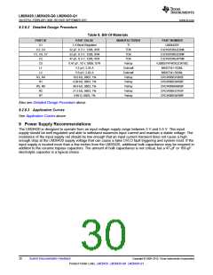
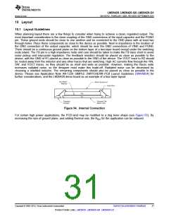
Figure 54. Internal Connection
For certain high power applications, the PCB land may be modified to a dog bone shape (see Figure 55). By
increasing the size of ground plane, and adding thermal vias, the RθJA for the application can be reduced.
Copyright © 2009–2015, Texas Instruments Incorporated
Submit Documentation Feedback
31
Product Folder Links: LM26420 LM26420-Q0 LM26420-Q1

 TI [ TEXAS INSTRUMENTS ]