LM26420, LM26420-Q0, LM26420-Q1
SNVS579J –FEBRUARY 2009–REVISED SEPTEMBER 2015
www.ti.com
IQ is the quiescent operating current, and is typically around 8.4 mA (IQVINC = 4.7 mA + IQVIND = 3.7 mA) for the
550-kHz frequency option.
Due to Dead-Time-Control Logic in the converter, there is a small delay (~4 nsec) between the turn ON and OFF
of the TOP and BOTTOM FET. During this time, the body diode of the BOTTOM FET is conducting with a
voltage drop of VBDIODE (~0.65 V). This allows the inductor current to circulate to the output, until the BOTTOM
FET is turned ON and the inductor current passes through the FET. There is a small amount of power loss due
to this body diode conducting and it can be calculated as follows:
PBDIODE = 2 × (VBDIODE × IOUT × FSW × TBDIODE
)
(32)
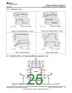
Typical Application power losses are:
PLOSS = ΣPCOND + PSW + PBDIODE + PIND + PQ
PINTERNAL = ΣPCOND + PSW+ PBDIODE + PQ
(33)
(34)
Table 3. Power Loss Tabulation
DESIGN PARAMETER
VALUE
5 V
DESIGN PARAMETER
VALUE
1.2 V
VIN
IOUT
VOUT
POUT
2 A
2.4 W
FSW
550 kHz
0.65 V
8.4 mA
1.5 nsec
1.5 nsec
75 mΩ
55 mΩ
20 mΩ
0.262
VBDIODE
IQ
PBDIODE
PQ
5.7 mW
42 mW
4.1 mW
4.1 mW
81 mW
167 mW
80 mW
384 mW
304 mW
TRISE
TFALL
RDSON_TOP
RDSON_BOT
INDDCR
D
PSWR
PSWF
PCOND_TOP
PCOND_BOT
PIND
PLOSS
η
86.2%
PINTERNAL
These calculations assume a junction temperature of 25°C. The RDSON values will be larger due to internal
heating; therefore, the internal power loss (PINTERNAL) must be first calculated to estimate the rise in junction
temperature.
24
Submit Documentation Feedback
Copyright © 2009–2015, Texas Instruments Incorporated
Product Folder Links: LM26420 LM26420-Q0 LM26420-Q1

 TI [ TEXAS INSTRUMENTS ]