LM2587
www.ti.com
SNVS115D –APRIL 2000–REVISED APRIL 2013
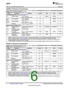
LM2587-ADJ Electrical Characteristics
Specifications with standard type face are for TJ = 25°C, and those in bold type face apply over full Operating Temperature
Range. Unless otherwise specified, VIN = 5V.
Symbol
Parameters
Conditions
Typical
Min
Max
Units
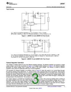
SYSTEM PARAMETERS Test Circuit of Figure 8(1)
VOUT
Output Voltage
Line Regulation
Load Regulation
Efficiency
VIN = 4V to 10V
ILOAD = 300 mA to 1.2A
12.0
20
11.52/11.40
12.48/12.60
100/200
V
ΔVOUT
ΔVIN
/
/
VIN = 4V to 10V
ILOAD = 300 mA
mV
mV
%
ΔVOUT
ΔILOAD
VIN = 10V
ILOAD = 300 mA to 1.2A
20
100/200
η
VIN = 10V, ILOAD = 1A
90
UNIQUE DEVICE PARAMETERS(2)
VREF
ΔVREF
GM
Output Reference
Voltage
Measured at Feedback Pin
VCOMP = 1.0V
1.230
1.5
1.208/1.205
1.252/1.255
6.000
V
mV
Reference Voltage
Line Regulation
VIN = 4V to 40V
Error Amp
Transconductance
ICOMP = −30 μA to +30 μA
VCOMP = 1.0V
3.200
670
1.800
mmho
V/V
nA
AVOL
IB
Error Amp
Voltage Gain
VCOMP = 0.5V to 1.6V
400/200
RCOMP = 1.0 MΩ(3)
Error Amp
VCOMP = 1.0V
125
425/600
Input Bias Current
(1) External components such as the diode, inductor, input and output capacitors can affect switching regulator performance. When the
LM2587 is used as shown in Figure 7 and Figure 8, system performance will be as specified by the system parameters.
(2) All room temperature limits are 100% production tested, and all limits at temperature extremes are specified via correlation using
standard Statistical Quality Control (SQC) methods.
(3) A 1.0 MΩ resistor is connected to the compensation pin (which is the error amplifier output) to ensure accuracy in measuring AVOL
.
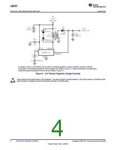
All Output Voltage Versions Electrical Characteristics(1)
Specifications with standard type face are for TJ = 25°C, and those in bold type face apply over full Operating Temperature
Range. Unless otherwise specified, VIN = 5V.
Symbol
IS
Parameters
Conditions
Typical
Min
Max
Units
Input Supply Current
(Switch Off)
See(2)
11
15.5/16.5
mA
ISWITCH = 3.0A
85
140/165
mA
V
VUV
fO
Input Supply
Undervoltage Lockout
RLOAD = 100Ω
3.30
3.05
3.75
Oscillator Frequency
Measured at Switch Pin
RLOAD = 100Ω
100
85/75
115/125
kHz
VCOMP = 1.0V
fSC
Short-Circuit
Frequency
Measured at Switch Pin
RLOAD = 100Ω
25
2.8
kHz
V
VFEEDBACK = 1.15V
VEAO
Error Amplifier
Output Swing
Upper Limit
See(3)
2.6/2.4
110/70
Lower Limit
See(2)
See(4)
0.25
0.40/0.55
260/320
V
IEAO
Error Amp
Output Current
(Source or Sink)
165
μA
(1) All room temperature limits are 100% production tested, and all limits at temperature extremes are specified via correlation using
standard Statistical Quality Control (SQC) methods.
(2) To measure this parameter, the feedback voltage is set to a high value, depending on the output version of the device, to force the error
amplifier output low. Adj: VFB = 1.41V; 3.3V: VFB = 3.80V; 5.0V: VFB = 5.75V; 12V: VFB = 13.80V.
(3) To measure this parameter, the feedback voltage is set to a low value, depending on the output version of the device, to force the error
amplifier output high. Adj: VFB = 1.05V; 3.3V: VFB = 2.81V; 5.0V: VFB = 4.25V; 12V: VFB = 10.20V.
(4) To measure the worst-case error amplifier output current, the LM2587 is tested with the feedback voltage set to its low value (specified
in Note 7) and at its high value (specified in Note 8).
Copyright © 2000–2013, Texas Instruments Incorporated
Submit Documentation Feedback
7
Product Folder Links: LM2587

 TI [ TEXAS INSTRUMENTS ]