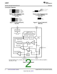
LM2587
www.ti.com
SNVS115D –APRIL 2000–REVISED APRIL 2013
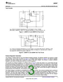
Test Circuits
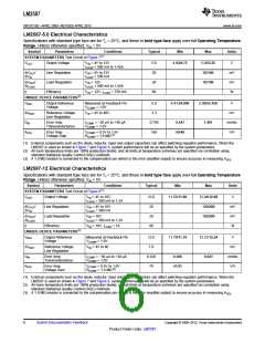
CIN1—100 μF, 25V Aluminum Electrolytic CIN2—0.1 μF CeramicT—22 μH, 1:1 Schott
#67141450D—1N5820COUT—680 μF, 16V Aluminum Electrolytic CC—0.47 μF Ceramic RC—2k
Figure 7. LM2587-3.3 and LM2587-5.0 Test Circuit
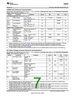
CIN1—100 μF, 25V Aluminum Electrolytic CIN2—0.1 μF CeramicL—15 μH, Renco #RL-5472-5D—1N5820COUT—680
μF, 16V Aluminum Electrolytic CC—0.47 μF Ceramic RC—2kFor 12V Devices: R1 = Short (0Ω) and R2 = Open For
ADJ Devices: R1 = 48.75k, ±0.1% and R2 = 5.62k, ±1%
Figure 8. LM2587-12 and LM2587-ADJ Test Circuit
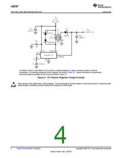
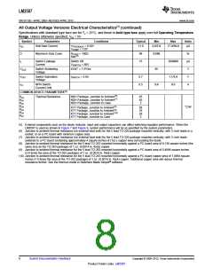
Flyback Regulator Operation
The LM2587 is ideally suited for use in the flyback regulator topology. The flyback regulator can produce a single
output voltage, such as the one shown in Figure 9, or multiple output voltages. In Figure 9, the flyback regulator
generates an output voltage that is inside the range of the input voltage. This feature is unique to flyback
regulators and cannot be duplicated with buck or boost regulators.
The operation of a flyback regulator is as follows (refer to Figure 9): when the switch is on, current flows through
the primary winding of the transformer, T1, storing energy in the magnetic field of the transformer. Note that the
primary and secondary windings are out of phase, so no current flows through the secondary when current flows
through the primary. When the switch turns off, the magnetic field collapses, reversing the voltage polarity of the
primary and secondary windings. Now rectifier D1 is forward biased and current flows through it, releasing the
energy stored in the transformer. This produces voltage at the output.
The output voltage is controlled by modulating the peak switch current. This is done by feeding back a portion of
the output voltage to the error amp, which amplifies the difference between the feedback voltage and a 1.230V
reference. The error amp output voltage is compared to a ramp voltage proportional to the switch current (i.e.,
inductor current during the switch on time). The comparator terminates the switch on time when the two voltages
are equal, thereby controlling the peak switch current to maintain a constant output voltage.
Copyright © 2000–2013, Texas Instruments Incorporated
Submit Documentation Feedback
3
Product Folder Links: LM2587

 TI [ TEXAS INSTRUMENTS ]