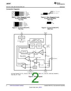
LM2587
SNVS115D –APRIL 2000–REVISED APRIL 2013
www.ti.com
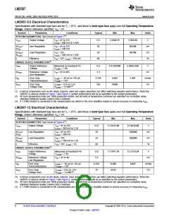
LM2587-5.0 Electrical Characteristics
Specifications with standard type face are for TJ = 25°C, and those in bold type face apply over full Operating Temperature
Range. Unless otherwise specified, VIN = 5V.
Symbol
Parameters
Conditions
Typical
Min
Max
Units
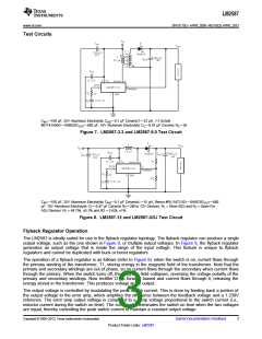
SYSTEM PARAMETERS Test Circuit of Figure 7(1)
VOUT
Output Voltage
Line Regulation
Load Regulation
Efficiency
VIN = 4V to 12V
ILOAD = 500 mA to 1.45A
5.0
20
20
80
4.80/4.75
5.20/5.25
50/100
V
ΔVOUT
ΔVIN
/
/
VIN = 4V to 12V
ILOAD = 500 mA
mV
mV
%
ΔVOUT
ΔILOAD
VIN = 12V
ILOAD = 500 mA to 1.45A
50/100
η
VIN = 12V, ILOAD = 750 mA
UNIQUE DEVICE PARAMETERS(2)
VREF
ΔVREF
GM
Output Reference
Voltage
Measured at Feedback Pin
VCOMP = 1.0V
5.0
3.3
4.913/4.900
5.088/5.100
V
Reference Voltage
Line Regulation
VIN = 4V to 40V
mV
Error Amp
Transconductance
ICOMP = −30 μA to +30 μA
VCOMP = 1.0V
0.750
165
0.447
1.491
mmho
V/V
AVOL
Error Amp
Voltage Gain
VCOMP = 0.5V to 1.6V
99/49
RCOMP = 1.0 MΩ(3)
(1) External components such as the diode, inductor, input and output capacitors can affect switching regulator performance. When the
LM2587 is used as shown in Figure 7 and Figure 8, system performance will be as specified by the system parameters.
(2) All room temperature limits are 100% production tested, and all limits at temperature extremes are specified via correlation using
standard Statistical Quality Control (SQC) methods.
(3) A 1.0 MΩ resistor is connected to the compensation pin (which is the error amplifier output) to ensure accuracy in measuring AVOL
.
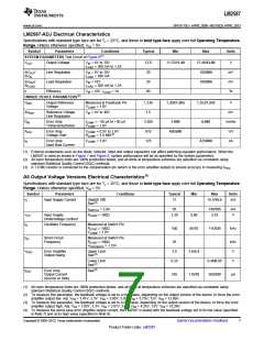
LM2587-12 Electrical Characteristics
Specifications with standard type face are for TJ = 25°C, and those in bold type face apply over full Operating Temperature
Range. Unless otherwise specified, VIN = 5V.
Symbol
Parameters
Conditions
Typical
Min
Max
Units
SYSTEM PARAMETERS Test Circuit of Figure 8(1)
VOUT
Output Voltage
Line Regulation
Load Regulation
Efficiency
VIN = 4V to 10V
ILOAD = 300 mA to 1.2A
12.0
20
11.52/11.40
12.48/12.60
100/200
V
ΔVOUT
ΔVIN
/
/
VIN = 4V to 10V
ILOAD = 300 mA
mV
mV
%
ΔVOUT
ΔILOAD
VIN = 10V
ILOAD = 300 mA to 1.2A
20
100/200
η
VIN = 10V, ILOAD = 1A
90
UNIQUE DEVICE PARAMETERS(2)
VREF
ΔVREF
GM
Output Reference
Voltage
Measured at Feedback Pin
VCOMP = 1.0V
12.0
7.8
11.79/11.76
12.21/12.24
V
Reference Voltage
Line Regulation
VIN = 4V to 40
mV
Error Amp
Transconductance
ICOMP = −30 μA to +30 μA
VCOMP = 1.0V
0.328
70
0.186
0.621
mmho
V/V
AVOL
Error Amp
Voltage Gain
VCOMP = 0.5V to 1.6V
41/21
RCOMP = 1.0 MΩ(3)
(1) External components such as the diode, inductor, input and output capacitors can affect switching regulator performance. When the
LM2587 is used as shown in Figure 7 and Figure 8, system performance will be as specified by the system parameters.
(2) All room temperature limits are 100% production tested, and all limits at temperature extremes are specified via correlation using
standard Statistical Quality Control (SQC) methods.
(3) A 1.0 MΩ resistor is connected to the compensation pin (which is the error amplifier output) to ensure accuracy in measuring AVOL
.
6
Submit Documentation Feedback
Copyright © 2000–2013, Texas Instruments Incorporated
Product Folder Links: LM2587

 TI [ TEXAS INSTRUMENTS ]