INA282, INA283
INA284, INA285
INA286
SBOS485A –NOVEMBER 2009–REVISED JULY 2010
www.ti.com
REFERENCE PIN CONNECTION OPTIONS
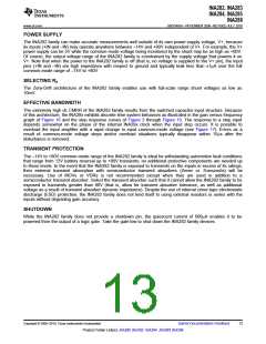
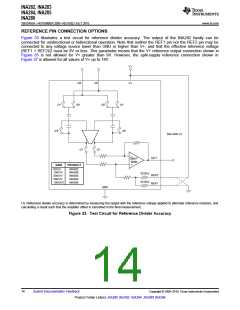
Figure 33 illustrates a test circuit for reference divider accuracy. The output of the INA282 family can be
connected for unidirectional or bidirectional operation. Note that neither the REF1 pin nor the REF2 pin may be
connected to any voltage source lower than GND or higher than V+, and that the effective reference voltage
(REF1 + REF2)/2 must be 9V or less. This parameter means that the V+ reference output connection shown in
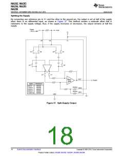
Figure 35 is not allowed for V+ greater than 9V. However, the split-supply reference connection shown in
Figure 37 is allowed for all values of V+ up to 18V.
V+
+IN
-IN
V+
Æ1
Æ2
Æ2
Æ1
Æ2
Æ2
See Note (1)
Æ1
Æ1
OUT
ZerÆ-
Drift
GAIN
PRODUCT
50V/V
INA282
INA286
INA283
INA284
INA285
100V/V
200V/V
500V/V
1000V/V
33.3kW
33.3kW
REF2
REF1
GND
(1) Reference divider accuracy is determined by measuring the output with the reference voltage applied to alternate reference resistors, and
calculating a result such that the amplifier offset is cancelled in the final measurement.
Figure 33. Test Circuit for Reference Divider Accuracy
14
Submit Documentation Feedback
Copyright © 2009–2010, Texas Instruments Incorporated
Product Folder Link(s): INA282 INA283 INA284 INA285 INA286

 TI [ TEXAS INSTRUMENTS ]