INA282, INA283
INA284, INA285
INA286
www.ti.com
SBOS485A –NOVEMBER 2009–REVISED JULY 2010
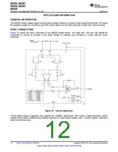
POWER SUPPLY
The INA282 family can make accurate measurements well outside of its own power-supply voltage, V+, because
its inputs (+IN and –IN) may operate anywhere between –14V and +80V independent of V+. For example, the V+
power supply can be 5V while the common-mode voltage being monitored by the shunt may be as high as +80V.
Of course, the output voltage range of the INA282 family is constrained by the supply voltage that powers it on
V+. Note that when the power to the INA282 family is off (that is, no voltage is supplied to the V+ pin), the input
pins (+IN and –IN) are high impedance with respect to ground and typically leak less than ±1mA over the full
common-mode range of –14V to +80V
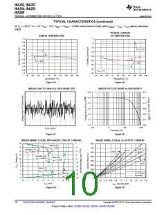
SELECTING RS
The Zerø-Drift architecture of the INA282 family enables use with full-scale range shunt voltages as low as
10mV.
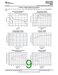
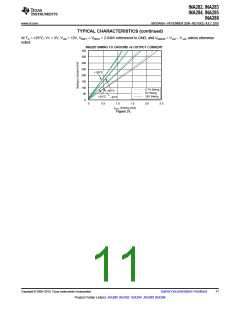
EFFECTIVE BANDWIDTH
The extremely high dc CMRR of the INA282 family results from the switched capacitor input structure. Because
of this architecture, the INA28x exhibits discrete time system behaviors as illustrated in the gain versus frequency
graph of Figure 16 and the step response curves of Figure 3 through Figure 10. The response to a step input
depends somewhat on the phase of the internal INA28x clock when the input step occurs. It is possible to
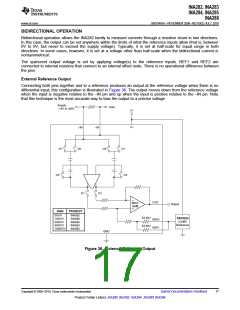
overload the input amplifier with a rapid change in input common-mode voltage (see Figure 17). Errors as a
result of common-mode voltage steps and/or overload situations typically disappear within 15ms after the
disturbance is removed.
TRANSIENT PROTECTION
The –14V to +80V common-mode range of the INA282 family is ideal for withstanding automotive fault conditions
that range from 12V battery reversal up to +80V transients; no additional protective components are needed up
to those levels. In the event that the INA282 family is exposed to transients on the inputs in excess of its ratings,
then external transient absorption with semiconductor transient absorbers (Zener or Transzorbs) will be
necessary. Use of MOVs or VDRs is not recommended except when they are used in addition to a
semiconductor transient absorber. Select the transient absorber such that it cannot allow the INA282 family to be
exposed to transients greater than 80V (that is, allow for transient absorber tolerance, as well as additional
voltage as a result of transient absorber dynamic impedance). Despite the use of internal zener-type electrostatic
discharge (ESD) protection, the INA282 family does not lend itself to using external resistors in series with the
inputs without degrading gain accuracy.
SHUTDOWN
While the INA282 family does not provide a shutdown pin, the quiescent current of 600mA enables it to be
powered from the output of a logic gate. Take the gate low to shut down the INA282 family devices.
Copyright © 2009–2010, Texas Instruments Incorporated
Submit Documentation Feedback
13
Product Folder Link(s): INA282 INA283 INA284 INA285 INA286

 TI [ TEXAS INSTRUMENTS ]
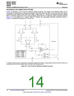
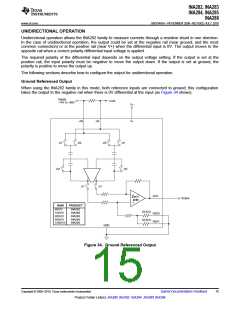
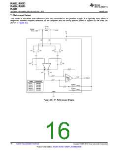