Applications Information
Power Up Sequence
and placement of external bypass capacitors less critical. This
practice is easier to implement in dense pcbs with many lay-
ers and may not be practical in simpler boards. External
bypass capacitors should include both RF ceramic and tan-
talum electrolytic types. RF capacitors may use values in the
range of 0.01 uF to 0.1 uF. Tantalum capacitors may be in the
2.2 uF to 10 uF range. Voltage rating of the tantalum capac-
itors should be at least 5X the power supply voltage being
used.
The VDD power supply pins do not require a specific power on
sequence and can be powered on in any order. However, the
PDB pin should only be set to logic HIGH once the power sent
to all supply pins is stable. Active clock and data inputs should
not be applied to the DS90C187 until all of the input power
pins have been powered on, settled to the recommended op-
erating voltage and the PDB pin has be set to logic HIGH..
The user experience can be impacted by the way a system
powers up and powers down an LCD screen. The following
sequence is recommended:
Surface mount capacitors are recommended due to their
smaller parasitics. When using multiple capacitors per supply
pin, locate the smaller value closer to the pin. It is recom-
mended to connect power and ground pins directly to the
power and ground planes with bypass capacitors connected
to the plane with vias on both ends of the capacitor.
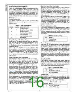
Power up sequence (DS90C187 PDB input initially LOW):
1. Ramp up LCD power (maybe 0.5ms to 10ms) but keep
backlight turned off.
2. Wait for additional 0-200ms to ensure display noise won’t
occur.
A small body size X7R chip capacitor, such as 0603, is rec-
ommended for external bypass. Its small body size reduces
the parasitic inductance of the capacitor. The user must pay
attention to the resonance frequency of these external bypass
capacitors, usually in the range of 20-30 MHz. To provide ef-
fective bypassing, multiple capacitors are often used to
achieve low impedance between the supply rails over the fre-
quency of interest. At high frequency, it is also a common
practice to use two vias from power and ground pins to the
planes, reducing the impedance at high frequency. Some de-
vices provide separate power and ground pins for different
portions of the circuit. This is done to isolate switching noise
effects between different sections of the circuit. Separate
planes on the PCB are typically not required. Pin Description
tables typically provide guidance on which circuit blocks are
connected to which power pin pairs. In some cases, an ex-
ternal filter many be used to provide clean power to sensitive
circuits such as PLLs.
3. Toggle DS90C187 power down pin to PDB = VIH.
4. Enable video source output; start sending black video
data.
5. Send >1ms of black video data; this allows the
DS90C187 to be phase locked, and the display to show
black data first.
6. Start sending true image data.
7. Enable backlight.
Power Down sequence (DS90C187 PDB input initially HIGH):
1. Disable LCD backlight; wait for the minimum time
specified in the LCD data sheet for the backlight to go
low.
2. Video source output data switch from active video data
to black image data (all visible pixel turn black); drive this
for >2 frame times.
Use at least a four layer board with a power and ground plane.
Locate LVCMOS signals away from the LVDS lines to prevent
coupling from the LVCMOS lines to the LVDS lines. Closely
coupled differential lines of 100 Ohms are typically recom-
mended for LVDS interconnect. The closely coupled lines
help to ensure that coupled noise will appear as common
mode and thus is rejected by the receivers. The tightly cou-
pled lines will also radiate less.
3. Set DS90C187 power down pin to PDB = GND.
4. Disable the video output of the video source.
5. Remove power from the LCD panel for lowest system
power.
Power Supply Filtering
The DS90C187 has several power supply pins at 1.8V. It is
important that these pins all be connected and properly by-
passed. Bypassing should consist of at least one 0.1μF ca-
pacitor placed on each pin, with an additional 4.7μF – 22μF
capacitor placed on the PLL supply pin (VDDPLL). 0.01μF
capacitors are typically recommended for each pin. Additional
filtering including ferrite beads may be necessary for noisy
systems. It is recommended to place a 0 ohm resistor at the
bypass capacitors that connect to each power pin to allow for
additional filtering if needed. A large bulk capacitor is recom-
mended at the point of power entry. This is typically in the
50μF — 100μF range.
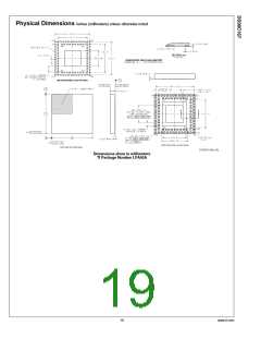
Information on the QFN (LLP) style package is provided in
Application Note: AN-1187.
LVDS Interconnect Guidelines
See AN-1108 and AN-905 for full details.
•
•
•
•
Use 100Ω coupled differential pairs
Use differential connectors when above 500Mbps
Minimize skew within the pair
Use the S/2S/3S rule in spacings
S = space between the pairs
2S = space between pairs
—
—
—
Layout Guidelines
3S = space to LVCMOS signals
Circuit board layout and stack-up for the LVDS serializer de-
vices should be designed to provide low-noise power feed to
the device. Good layout practice will also separate high fre-
quency or high-level inputs and outputs to minimize unwanted
stray noise pickup, feedback and interference. Power system
performance may be greatly improved by using thin di-
electrics (2 to 4 mils) for power / ground sandwiches. This
arrangement provides plane capacitance for the PCB power
system with low-inductance parasitics, which has proven es-
pecially effective at high frequencies, and makes the value
•
•
Place ground vias next to signal vias when changing
between layers
When a signal changes reference planes, place a bypass
cap and vias between the new and old reference plane
For more tips and detailed suggestions regarding high speed
board layout principles, please consult the LVDS Owner's
Manual at: http://www.ti.com/lvds
www.ti.com
18

 TI [ TEXAS INSTRUMENTS ]