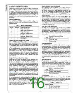
Any unused LVDS outputs that are not powered down or put
into TRI-STATE® due to the MODE0, MODE1, or 18B pins
should be externally terminated differentially with a 100 ohm
resistor. For example, when driving a timing controller
(TCON) that only requires an 8D + C LVDS interface, rather
than 8D + 2C, the unused clock line should be terminated near
the package of the DS90C187. For more information regard-
ing the output state of unused LVDS drivers, refer to the next
section, 18 bit / 24 bit Color Mode (18B). For more information
regarding the electrical characteristics of the LVDS outputs,
refer to the LVDS DC Characteristics and LVDS Switching
Specifications.
function. So if the device is configured for 18 bit color Single
Pixel In/Single Pixel Out, LVDS channel OB_3+/- will be pow-
ered down and not TRI-STATE®. If an LVDS driver is pow-
ered down, each output terminal is pulled low by a 100 ohm
resistor to ground.
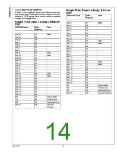
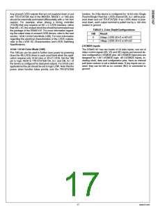
TABLE 5. Color DepthConfigurations
18B
0
Result
24bpp, LVDS 4D+C or 8D+2C
18bpp, LVDS 3D+C or 6D+2C
1
LVCMOS Inputs
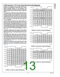
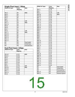
18 bit / 24 bit Color Mode (18B)
The DS90C187 has two banks of 24 data inputs, one set of
video control signal (HS, VS and DE) inputs and several de-
vice configuration LVCMOS pins. All LVCMOS input pins are
designed for 1.8V LVCMOS logic. All LVCMOS inputs, in-
cluding clock, data and configuration pins, have an internal
pull down resistor to set a default state. If any inputs are un-
used, they can be left as no connect (NC) or connected to
ground.
The 18B pin can be used to further save power by powering
down the 4th LVDS driver in each used bank when the appli-
cation requires only 18 bit color or 3D+C LVDS. Set the 18B
pin to logic HIGH to TRI-STATE® OA_3+/- and OB_3+/- (if
the device is configured for dual pixel output). For 24 bit color
applications this pin should be set to logic LOW. Note that the
power down function takes priority over the TRI-STATE®
17
www.ti.com

 TI [ TEXAS INSTRUMENTS ]