LVDS Interface / TFT Color Data Recommended Mapping
Different color mapping options exist. Check with the color
mapping of the Deserializer / TCON device that is used to
ensure compatible mapping for the application. The
DS90C187 supports three modes of operation for single and
dual pixel applications supporting either 24bpp or 18bpp color
depths.
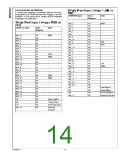
In the Dual Pixel / 24bpp mode, eight LVDS data lines are
provided along with two LVDS clock lines (8D+2C). The De-
serializer may utilize one or two clock lines. The 53 bit inter-
face typically assigns 24 bits to RGB for the odd pixel, 24 bits
to RGB for the even pixel, 3 bits for the video control signals
(HS, VS and DE), 1 bit for odd pixel and 1 bit for even pixel
which can be ignored or used for general purpose data, con-
trol or L/R signaling.
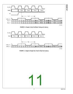
A reduced width input interface is also supported with a Sin-
gle-to-Dual Pixel conversion where the data is presented at
double rate (same clock edge, 2X speed, see Figure 10) and
the DE transition is used is flag the first pixel. Also note in both
8D+2C configurations, the three video control signals are sent
over both the A and B outputs. The DES / TCON may recover
one set, or both depending upon its implementation. The Dual
Pixel / 24bpp 8D+2C LVDS Interface Mapping is shown in
Figure 14.
30151677
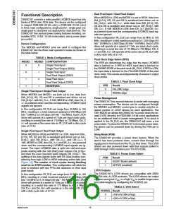
A Dual Pixel / 18bpp mode is also supported. In this configu-
FIGURE 15. Dual Pixel / 18bpp LVDS Mapping
ration OA3 and OB3 LVDS output channels are placed in TRI-
STATE® to save power. Their respective inputs are ignored.
(Figure 15)
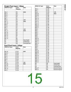
In the Single Pixel / 24bpp mode, four LVDS data lines are
provided along with a LVDS clock line (4D+C). The 28 bit in-
terface typically assigns 24 bits to RGB color data, 3 bits to
video control (HS, VS and DE) and one spare bit can be ig-
nored, used for L/R signaling or function as a general purpose
bit. The Single Pixel / 24bpp 4D+C LVDS Interface Mapping
is shown in Figure 16.
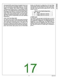
A Single Pixel / 18bpp mode is also supported. In this config-
uration the OA3 LVDS output channel is placed in TRI-
STATE® to save power. Its respective inputs are ignored.
(Figure 17)
30151679
FIGURE 16. Single Pixel / 24bpp LVDS Mapping
30151678
FIGURE 17. Single Pixel / 18bpp LVDS Mapping
30151676
FIGURE 14. Dual Pixel / 24bpp LVDS Mapping
13
www.ti.com

 TI [ TEXAS INSTRUMENTS ]