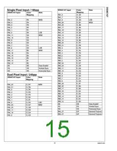
Dual Pixel Input / Dual Pixel Output
Functional Description
When MODE0 is LOW and MODE1 is set to HIGH, data from
INA_[27:0], HS, VS and DE is serialized and driven out on
OA_[3:0]+/- with OA_C+/-, while data from INB_[27:0], HS,
VS and DE is serializer and driven out on OB_[3:0]+/- with
OB_C+/-. If 18B_MODE is LOW, then OA_3+/- and OB_3+/-
is powered down and the corresponding LVCMOS input sig-
nals are ignored.
DS90C187 converts a wide parallel LVCMOS input bus into
banks of FPD-Link LVDS data. The device can be configured
to support RGB-888 (24 bit color) or RGB-666 (18 bit color)
in three main configurations: single pixel in / single pixel out;
single pixel in / dual pixel out; dual pixel in / dual pixel out. The
DS90C187 has several power saving features including: se-
lectable VOD, 18 bit / 24 bit mode select, and a power down
pin control.
In this configuration IN_CLK can range from 25 MHz to 105
MHz, resulting in a total maximum payload of 1.325 Gbps (53
bits * 25 MHz) to 5.565 Gbps (53 bits * 105 MHz). Each LVDS
driver will operate at a speed of 7 bits per input clock cycle,
resulting in a serial line rate of 175 Mbps to 735 Mbps. OA_C
+/- and OB_C+/- will operate at the same rate as IN_CLK with
a duty cycle ratio of 57:43.
Device Configuration
The MODE0 and MODE1 pins are used to configure the
DS90C187 into the three main operation modes as shown in
the table below.
TABLE 1. Mode Configurations
Pixel Clock Edge Select (RFB)
MODE1
MODE0 CONFIGURATION
The RFB pin determines the edge that the input LVCMOS
data is latched on. If RFB is HIGH, input data is latched on
the RISING EDGE of the pixel clock (IN_CLK). If RFB is LOW,
the input data is latched on the FALLING EDGE of the pixel
clock. Note: This can be set independently of receiver’s output
clock strobe.
0
0
1
0
1
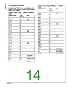
Single Pixel Input /
Single Pixel Output (SISO)
0
1
1
Single Pixel Input /
Dual Pixel Output (SIDO)
Dual Pixel Input /
Dual Pixel Output (DIDO)
TABLE 2. Pixel Clock Edge
RFB
Result
RESERVED
0
1
FALLING edge
RISING edge
Single Pixel Input / Single Pixel Output
When MODE0 and MODE1 are both set to low, data from
INA_[27:0], HS, VS and DE is serialized and driven out on
OA_[3:0]+/- with OA_C+/-. If 18B_MODE is LOW, then OA_3
+/- is powered down and the corresponding LVCMOS input
signals are ignored.
Power Management
The DS90C187 has several features to assist with managing
power consumption. The device can be configured through
the MODE0 and MODE1 control pins to enable only the re-
quired number of LVDS drivers for each application. The
18B_MODE pin allows the DS90C187 to power down the un-
used LVDS driver(s) for RGB-666 (18 bit color) applications
for an additional level of power management. If no clock is
applied to the IN_CLK pin, the DS90C187 will enter a low
power state. To place the DS90C187 in its lowest power state,
the device can be powered down by driving the PDB pin to
LOW.
In this configuration IN_CLK can range from 25 MHz to 105
MHz, resulting in a total maximum payload of 700 Mbps (28
bits * 25MHz) to 2.94 Gbps (28 bits * 105 MHz). Each LVDS
driver will operate at a speed of 7 bits per input clock cycle,
resulting in a serial line rate of 175 Mbps to 735 Mbps. OA_C
+/- will operate at the same rate as IN_CLK with a duty cycle
ratio of 57:43.
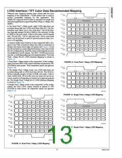
Single Pixel Input / Dual Pixel Output
When MODE0 is HIGH and MODE1 is LOW, data from INA_
[27:0], HS, VS and DE is serialized and driven out on OA_
[3:0]+/- and OB_[3:0]+/- with OA_C+/- and OB_C+/-. If
18B_MODE is LOW, then OA_3+/- and OB_3+/- are powered
down and the corresponding LVCMOS input signals are ig-
nored. The input LVCMOS data is split into odd and even
pixels starting with the odd (first) pixel outputs OA_[3:0]+/-
and then the even (second) pixel outputs OB_[3:0]+/-. The
splitting of the data signals starts with DE (data enable) tran-
sitioning from logic LOW to HIGH indicating active data (see
Figure 10). The number of clock cycles during blanking
must be an EVEN number. This configuration will allow the
user to interface with two FPD-Link receivers or other dual
pixel inputs.
Sleep Mode (PDB)
The DS90C187 provides a power down feature. When the
device has been powered down, current draw through the
supply pins is minimized and the PLL is shut down. The LVDS
drivers are also powered down with their outputs pulled to
GND through 100Ω resistors (not TRI-STATE®).
TABLE 3. Power Down Select
PDB
Result
0
1
SLEEP Mode (default)
ACTIVE (enabled)
LVDS Outputs
The DS90C187's LVDS drivers are compatible with ANSI/
TIA/EIA-644–A LVDS receivers. The LVDS drivers can output
a power saving low VOD, or a high VOD to enable longer trace
and cable lengths by configuring the VODSEL pin.
In this configuration IN_CLK can range from 50 MHz to 185
MHz, resulting in a total maximum payload of 1.4 Gbps (28
bits * 50 MHz) to 5.18 Gbps (28 bits * 185 MHz). Each LVDS
driver will operate at a speed of 7 bits per 2 input clock cycles,
resulting in a serial line rate of 175 Mbps to 647.5 Mbps.
OA_C+/- and OA_B+/- will operate at ½ the rate as IN_CLK
with a duty cycle ratio of 57:43.
TABLE 4. VOD Select
VODSEL Result
0
1
±180 mV (360 mVpp)
±300 mV (600 mVpp)
www.ti.com
16

 TI [ TEXAS INSTRUMENTS ]