DRV8874
SLVSF66A –AUGUST 2019–REVISED DECEMBER 2019
www.ti.com
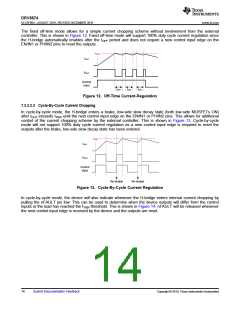
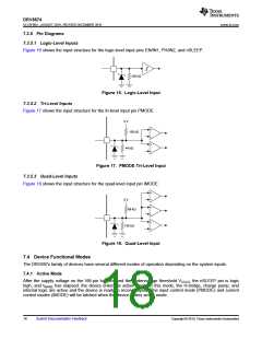
7.3.5 Pin Diagrams
7.3.5.1 Logic-Level Inputs
Figure 16 shows the input structure for the logic-level input pins EN/IN1, PH/IN2, and nSLEEP.
100 kꢀ
Figure 16. Logic-Level Input
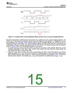
7.3.5.2 Tri-Level Inputs
Figure 17 shows the input structure for the tri-level input pin PMODE.
5 V
+
156 kꢀ
œ
+
44 kꢀ
œ
Figure 17. PMODE Tri-Level Input
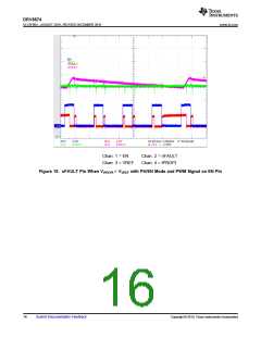
7.3.5.3 Quad-Level Inputs
Figure 18 shows the input structure for the quad-level input pin IMODE.
+
œ
5 V
+
68 kꢀ
œ
+
136 kꢀ
œ
Figure 18. Quad-Level Input
7.4 Device Functional Modes
The DRV887x family of devices have several different modes of operation depending on the system inputs.
7.4.1 Active Mode
After the supply voltage on the VM pin has crossed the undervoltage threshold VUVLO, the nSLEEP pin is logic
high, and tWAKE has elapsed, the device enters its active mode. In this mode, the H-bridge, charge pump, and
internal logic are active and the device is ready to receive inputs. The input control mode (PMODE) and current
control modes (IMODE) will be latched when the device enters active mode.
18
Submit Documentation Feedback
Copyright © 2019, Texas Instruments Incorporated

 TI [ TEXAS INSTRUMENTS ]