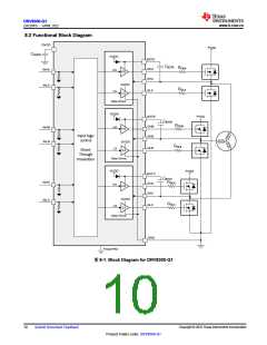
DRV8300-Q1
ZHCSPF5 –APRIL 2022
www.ti.com.cn
UNIT
7.4 Thermal Information
DRV8300-Q1
PW (TSSOP)
20 PINS
97.4
THERMAL METRIC (1)
RθJA
Junction-to-ambient thermal resistance
°C/W
°C/W
°C/W
°C/W
°C/W
°C/W
RθJC(top) Junction-to-case (top) thermal resistance
38.3
RθJB
ΨJT
Junction-to-board thermal resistance
48.8
Junction-to-top characterization parameter
Junction-to-board characterization parameter
4.3
48.4
ΨJB
RθJC(bot) Junction-to-case (bottom) thermal resistance
N/A
(1) For more information about traditional and new thermal metrics, see the Semiconductor and IC Package Thermal Metrics application
report.
7.5 Electrical Characteristics
4.8 V ≤VGVDD ≤20 V, –40°C ≤TJ ≤150°C (unless otherwise noted)
PARAMETER
TEST CONDITIONS
MIN
TYP
MAX
UNIT
POWER SUPPLIES (GVDD, BSTx)
GVDD standby mode current
INHx = INLX = 0; VBSTx = VGVDD
400
400
2
800
825
4
1400
1400
7
µA
µA
µA
µA
IGVDD
INHx = INLX = Switching @20kHz; VBSTx
= VGVDD; NO FETs connected
GVDD active mode current
Bootstrap pin leakage current
ILBSx
VBSTx = VSHx = 85V; VGVDD = 0V
INHx = Switching@20kHz
Bootstrap pin active mode transient
leakage current
ILBS_TRAN
30
105
220
Bootstrap pin active mode leakage
static current
ILBS_DC
ILSHx
INHx = High
30
30
85
55
150
80
µA
µA
INHx = INLX = 0; VBSTx - VSHx = 12V;
VSHx = 0 to 85V
High-side source pin leakage current
LOGIC-LEVEL INPUTS (INHx, INLx, MODE)
VHYS_MODE
VHYS
Input hysteresis
Input hysteresis
Mode pin
1600
40
2000
100
2400
260
mV
mV
INLx, INHx pins
VPIN (Pin Voltage) = 0 V; INLx in non-
inverting mode
IIL_INLx
IIH_INLx
INLx Input logic low current
INLx Input logic high current
-1
5
0
1
µA
µA
VPIN (Pin Voltage) = 5 V; INLx in non-
inverting mode
20
30
IIL
INHx, MODE Input logic low current VPIN (Pin Voltage) = 0 V;
INHx, MODE Input logic high current VPIN (Pin Voltage) = 5 V;
-1
5
0
20
1
30
µA
µA
IIH
RPD_INHx
RPD_INLx
RPD_MODE
INHx Input pulldown resistance
INLx Input pulldown resistance
MODE Input pulldown resistance
To GND
120
120
120
200
200
200
280
280
280
kΩ
kΩ
kΩ
To GND, INLx in non-inverting mode
To GND
GATE DRIVERS (GHx, GLx, SHx, SLx)
IGLx = -100 mA; VGVDD = 12V; No FETs
connected
VGHx_LO
VGHx_HI
VGLx_LO
VGLx_HI
High-side gate drive low level voltage
0
0.3
0
0.15
0.6
0.35
1.2
V
V
V
V
High-side gate drive high level
voltage (VBSTx - VGHx
IGHx = 100 mA; VGVDD = 12V; No FETs
connected
)
IGLx = -100 mA; VGVDD = 12V; No FETs
connected
Low-side gate drive low level voltage
0.15
0.6
0.35
1.2
Low-side gate drive high level voltage IGHx = 100 mA; VGVDD = 12V; No FETs
0.3
(VGVDD - VGHx
)
connected
IDRIVEP_HS
IDRIVEN_HS
High-side peak source gate current
High-side peak sink gate current
GHx-SHx = 12V
GHx-SHx = 0V
400
850
750
1200
2100
mA
mA
1500
Copyright © 2022 Texas Instruments Incorporated
6
Submit Document Feedback
Product Folder Links: DRV8300-Q1

 TI [ TEXAS INSTRUMENTS ]