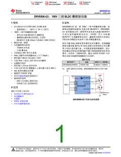
DRV8300-Q1
ZHCSPF5 –APRIL 2022
www.ti.com.cn
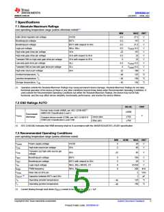
7 Specifications
7.1 Absolute Maximum Ratings
over operating temperature range (unless otherwise noted)(1)
MIN
-0.3
-0.3
-0.3
-0.3
-22
MAX UNIT
Gate driver regulator pin voltage
Bootstrap pin voltage
GVDD
21.5
115
V
V
BSTx
Bootstrap pin voltage
BSTx with respect to SHx
21.5
V
Logic pin voltage
INHx, INLx
VGVDD+0.3
115
V
High-side gate drive pin voltage
High-side gate drive pin voltage
Transient 500-ns high-side gate drive pin voltage
Low-side gate drive pin voltage
Transient 500-ns low-side gate drive pin voltage
High-side source pin voltage
Ambient temperature, TA
GHx
V
GHx with respect to SHx
-0.3
-5
22
V
GHx with respect to SHx
22
V
GLx
GLx
SHx
-0.3
-5
VGVDD+0.3
VGVDD+0.3
100
V
V
-22
V
125
°C
°C
°C
–40
–40
–65
Junction temperature, TJ
150
Storage temperature, Tstg
150
(1) Operation outside the Absolute Maximum Ratings may cause permanent device damage. Absolute Maximum Ratings do not imply
functional operation of the device at these or any other conditions beyond those listed under Recommended Operating Conditions. If
used outside the Recommended Operating Conditions but within the Absolute Maximum Ratings, the device may not be fully
functional, and this may affect device reliability, functionality, performance, and shorten the device lifetime
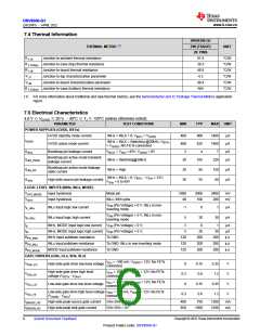
7.2 ESD Ratings AUTO
VALUE
UNIT
Human body model (HBM), per AEC Q100-002(1)
HBM ESD Classification Level 2
±2000
Electrostatic
discharge
V(ESD)
V
Corner pins
Other pins
±750
±750
Charged device model (CDM), per AEC Q100-011
CDM ESD Classification Level C4B
(1) AEC Q100-002 indicates that HBM stressing shall be in accordance with the ANSI/ESDA/JEDEC JS-001 specification.
7.3 Recommended Operating Conditions
over operating temperature range (unless otherwise noted)
MIN
5
NOM
MAX UNIT
VGVDD
VSHx
Power supply voltage
GVDD
SHx
20
85
V
V
High-side source pin voltage
-2
Transient 2µs high-side source pin
voltage
VSHx
SHx
-22
85
V
VBST
VBST
VIN
Bootstrap pin voltage
BSTx
5
5
0
0
105
20
V
V
Bootstrap pin voltage
BSTx with respect to SHx
INHx, INLx, MODE, DT
INHx, INLx
Logic input voltage
GVDD
200
2
V
fPWM
VSHSL
CBOOT
TA
PWM frequency
kHz
V/ns
µF
°C
°C
Slew rate on SHx pin
(1)
Capacitor between BSTx and SHx
Operating ambient temperature
Operating junction temperature
1
125
150
–40
–40
TJ
(1) Current flowing through boot diode (DBOOT) needs to be limited for CBOOT > 1µF
Copyright © 2022 Texas Instruments Incorporated
Submit Document Feedback
5
Product Folder Links: DRV8300-Q1

 TI [ TEXAS INSTRUMENTS ]