DRV8300-Q1
ZHCSPF5 –APRIL 2022
www.ti.com.cn
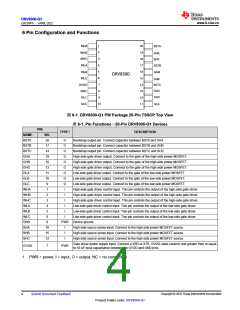
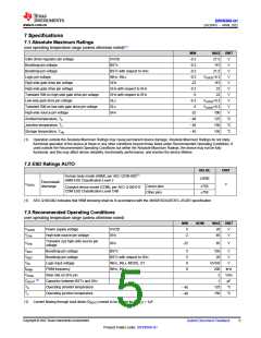
6 Pin Configuration and Functions
1
INHA
20
19
18
17
16
15
14
13
12
11
BSTA
2
3
4
5
6
INHB
INHC
GHA
SHA
BSTB
GHB
INLA
INLB
INLC
GVDD
GND
GLC
DRV8300
SHB
BSTC
GHC
7
8
SHC
GLA
9
GLB
10
图6-1. DRV8300-Q1 PW Package 20-Pin TSSOP Top View
表6-1. Pin Functions—20-Pin DRV8300-Q1 Devices
PIN
TYPE1
DESCRIPTION
NAME
BSTA
BSTB
BSTC
GHA
GHB
GHC
GLA
NO.
20
17
14
19
16
13
11
10
9
O
O
O
O
O
O
O
O
O
I
Bootstrap output pin. Connect capacitor between BSTA and SHA
Bootstrap output pin. Connect capacitor between BSTB and SHB
Bootstrap output pin. Connect capacitor between BSTC and SHC
High-side gate driver output. Connect to the gate of the high-side power MOSFET.
High-side gate driver output. Connect to the gate of the high-side power MOSFET.
High-side gate driver output. Connect to the gate of the high-side power MOSFET.
Low-side gate driver output. Connect to the gate of the low-side power MOSFET.
Low-side gate driver output. Connect to the gate of the low-side power MOSFET.
Low-side gate driver output. Connect to the gate of the low-side power MOSFET.
GLB
GLC
INHA
INHB
INHC
INLA
INLB
INLC
GND
SHA
1
High-side gate driver control input. This pin controls the output of the high-side gate driver.
High-side gate driver control input. This pin controls the output of the high-side gate driver.
High-side gate driver control input. This pin controls the output of the high-side gate driver.
Low-side gate driver control input. This pin controls the output of the low-side gate driver.
Low-side gate driver control input. This pin controls the output of the low-side gate driver.
Low-side gate driver control input. This pin controls the output of the low-side gate driver.
2
I
3
I
4
I
5
I
6
I
8
PWR Device ground.
18
15
12
I
I
I
High-side source sense input. Connect to the high-side power MOSFET source.
SHB
High-side source sense input. Connect to the high-side power MOSFET source.
High-side source sense input. Connect to the high-side power MOSFET source.
SHC
Gate driver power supply input. Connect a X5R or X7R, GVDD-rated ceramic and greater then or equal
to 10-uF local capacitance between the GVDD and GND pins.
GVDD
7
PWR
1. PWR = power, I = input, O = output, NC = no connection
Copyright © 2022 Texas Instruments Incorporated
4
Submit Document Feedback
Product Folder Links: DRV8300-Q1

 TI [ TEXAS INSTRUMENTS ]