DM385, DM388
www.ti.com
SPRS821D –MARCH 2013–REVISED DECEMBER 2013
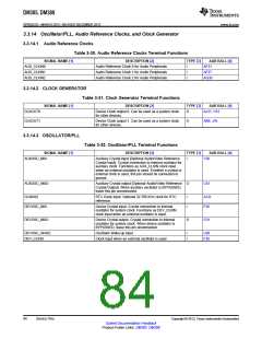
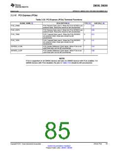
3.3.15 PCI Express (PCIe)
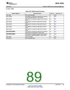
Table 3-33. PCI Express (PCIe) Terminal Functions
SIGNAL NAME [1]
DESCRIPTION [2]
TYPE [3]
AAR BALL [4]
PCIE_RXN0
PCIE_RXP0
PCIE_TXN0
PCIE Receive Data Lane 0. When the PCIe SERDES are
powered down, these pins should be left unconnected.
I
J30
PCIE Receive Data Lane 0. When the PCIe SERDES are
powered down, these pins should be left unconnected.
I
K30
K31
PCIE Transmit Data Lane 0. When the PCIe SERDES
are powered down, these pins should be left
unconnected.
O
PCIE_TXP0
PCIE Transmit Data Lane 0. When the PCIe SERDES
are powered down, these pins should be left
unconnected.
O
L31
SERDES_CLKN
SERDES_CLKP
PCIE Serdes Reference Clock Inputs. When PCIe is not
used these pins can be left unconnected.
I
I
H31
H30
PCIE Serdes Reference Clock Inputs. When PCIe is not
used these pins can be left unconnected.
NOTE
PCIe is supported on all DM385 devices and also on DM388 devices with PCIe enabled. For
DM388 devices with PCIe disabled, the pins in Table 3-33 should be left unconnected.
Copyright © 2013, Texas Instruments Incorporated
Device Pins
85
Submit Documentation Feedback
Product Folder Links: DM385 DM388

 TI [ TEXAS INSTRUMENTS ]